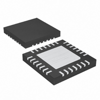
MAX8724ETI+T Maxim Integrated Products, MAX8724ETI+T Datasheet - Page 13

MAX8724ETI+T
Manufacturer Part Number
MAX8724ETI+T
Description
IC CHARGER BATTERY 28-TQFN
Manufacturer
Maxim Integrated Products
Datasheet
1.MAX1908ETI.pdf
(30 pages)
Specifications of MAX8724ETI+T
Function
Charge Management
Battery Type
Multi-Chemistry
Voltage - Supply
8 V ~ 28 V
Operating Temperature
-40°C ~ 85°C
Mounting Type
Surface Mount
Package / Case
28-WFQFN Exposed Pad
Lead Free Status / RoHS Status
Lead free / RoHS Compliant
PIN
10
11
12
13
14
15
16
17
18
19
20
21
22
23
24
25
26
27
28
1
2
3
4
5
6
7
8
9
CELLS
NAME
ACOK
REFIN
PGND
SHDN
DLOV
CSSN
ICHG
CSSP
Low-Cost Multichemistry Battery Chargers
DCIN
ACIN
VCTL
BATT
CSIN
GND
CSIP
LDO
CCS
CCV
ICTL
DLO
CLS
REF
BST
IINP
CCI
DHI
LX
______________________________________________________________________________________
Charging Voltage Input. Bypass DCIN with a 1µF capacitor to PGND.
D evi ce P ow er S up p l y. Outp ut of the 5.4V l i near r eg ul ator sup p l i ed fr om D C IN . Byp ass w i th a 1µF cap aci tor to GN D .
Source Current-Limit Input. Voltage input for setting the current limit of the input source.
4.096V Voltage Reference. Bypass REF with a 1µF capacitor to GND.
Input-Current Regulation Loop-Compensation Point. Connect a 0.01µF capacitor to GND.
Output-Current Regulation Loop-Compensation Point. Connect a 0.01µF capacitor to GND.
Voltage Regulation Loop-Compensation Point. Connect 1kΩ in series with a 0.1µF capacitor to GND.
Shutdown Control Input. Drive SHDN logic low to shut down the MAX1908/MAX8724/MAX8765 MAX8765A.
Use with a thermistor to detect a hot battery and suspend charging.
Charge-Current Monitor Output. ICHG is a scaled-down replica of the charger output current. Use ICHG to
monitor the charging current and detect when the chip changes from constant-current mode to constant-
voltage mode. The transconductance of (CSIP - CSIN) to ICHG is 3µA/mV.
AC Detect Input. Input to an uncommitted comparator. ACIN can be used to detect AC-adapter presence.
AC Detect Output. High-voltage open-drain output is high impedance when V
Reference Input. Allows the ICTL and VCTL inputs to have ratiometric ranges for increased accuracy.
Output Current-Limit Set Input. ICTL input voltage range is V
down if ICTL is forced below V
LDO, the set point for CSIP - CSIN is 45mV.
Analog Ground
Output Voltage-Limit Set Input. VCTL input voltage range is 0 to V
point is (4.2 x CELLS)V.
Battery Voltage Input
Cell Count Input. Tri-level input for setting number of cells. GND = 2 cells, open = 3 cells, REFIN = 4 cells.
Output Current-Sense Negative Input
Output Current-Sense Positive Input. Connect a current-sense resistor from CSIP to CSIN.
Power Ground
Low-Side Power MOSFET Driver Output. Connect to low-side nMOS gate.
Low-Side Driver Supply. Bypass DLOV with a 1µF capacitor to GND.
High-Side Power MOSFET Driver Power-Return Connection. Connect to the source of the high-side nMOS.
High-Side Power MOSFET Driver Power-Supply Connection. Connect a 0.1µF capacitor from LX to BST.
High-Side Power MOSFET Driver Output. Connect to high-side nMOS gate.
Input Current-Sense Negative Input
Input Current-Sense Positive Input. Connect a current-sense resistor from CSSP to CSSN.
Input-Current Monitor Output. IINP is a scaled-down replica of the input current. IINP monitors the total
system current. The transconductance of (CSSP - CSSN) to IINP is 3µA/mV.
REFIN
/100 while the MAX8765/MAX8765A does not. When ICTL is equal to
FUNCTION
REFIN
REFIN
/32 to V
. When VCTL is equal to LDO, the set
REFIN
ACIN
. The MAX1908/MAX8724 shut
Pin Description
is less than V
REF
/2.
13


