MAX8934AETI+ Maxim Integrated Products, MAX8934AETI+ Datasheet - Page 28
MAX8934AETI+
Manufacturer Part Number
MAX8934AETI+
Description
IC BATTERY CHARGER DUAL 28TQFN
Manufacturer
Maxim Integrated Products
Series
Smart Power Selector™r
Datasheet
1.MAX8934AETIT.pdf
(31 pages)
Specifications of MAX8934AETI+
Function
Charge Management
Battery Type
Lithium-Ion (Li-Ion), Lithium-Polymer (Li-Pol)
Voltage - Supply
4.1 V ~ 6.6 V
Operating Temperature
-40°C ~ 85°C
Mounting Type
Surface Mount
Package / Case
28-TQFN Exposed Pad
Product
Charge Management
Output Voltage
1 V
Operating Supply Voltage
4.1 V to 6.6 V
Supply Current
1 mA
Maximum Operating Temperature
+ 85 C
Minimum Operating Temperature
- 40 C
Charge Safety Timers
Yes
Mounting Style
SMD/SMT
Temperature Monitoring
Yes
Lead Free Status / RoHS Status
Lead free / RoHS Compliant


**For safety region 2, contact factory.
†For thermistor Beta = 3477, contact factory.
Dual-Input Linear Chargers, Smart Power Selector
with Advanced Battery Temperature Monitoring
The ultra-low quiescent current LDO is always on and is
preset to an output voltage of 3.3V. The LDO provides
up to 30mA output current. When DC and USB are inval-
id and the battery is discharging, the LDO output volt-
age tracks V
capacitor connected from LDO to GND is recommended
for most applications.
Table 3. Package Thermal Characteristics
28
MAX8934AETI+
MAX8934BETI+
MAX8934CETI+
MAX8934DETI+
MAX8934EETI+
Continuous
Dissipation
Power
_____________________________________________________________________________________
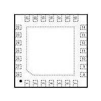
B
B
TOP VIEW
JA
JC
PART
CHG
DOK
UOK
SYS
SYS
FLT
OT
SYS
SINGLE-LAYER PCB
1666.7mW
(derate 20.8mW/NC
above +70NC)
48NC/W
3NC/W
*EXPOSED PAD
22
23
24
26
27
28
25
as it drops below 3.3V. A 1FF ceramic
21
28-PIN 4mm x 4mm THIN QFN
1
20
REGION**
2
SAFETY
THIN QFN
MAX8934A–
19
3
MAX8934E
1
1
1
1
1
Pin Configuration
18
4
17
5
Always-On LDO
*EP
MULTILAYER PCB
2286mW
(derate 28.6mW/NC
above +70NC)
35NC/W
3NC/W
16
6
SYS VOLTAGE (V)
15
7
14 THM
13 GND
12
11
10
9
8
4.35
4.35
4.35
4.35
5.3
USUS
ISET
CT
GND
V
L
THERMISTOR
+Denotes a lead(Pb)-free/RoHS-compliant package.
*EP = Exposed pad.
PROCESS: BiCMOS
Good design minimizes ground bounce and voltage
gradients in the ground plane. GND should connect to
the power-ground plane at only one point to minimize the
effects of power-ground currents. Battery ground should
connect directly to the power-ground plane. Connect
GND to the exposed pad directly under the IC. Use mul-
tiple tightly spaced vias to the ground plane under the
exposed pad to help cool the IC. Position input capaci-
tors from DC, SYS, BATT, and USB to the power-ground
plane as close as possible to the IC. Keep high current
traces such as those to DC, SYS, and BATT as short and
wide as possible. Refer to the MAX8934 Evaluation Kit
for a suitable PCB layout example.
MAX8934BETI+
MAX8934CETI+
MAX8934DETI+
MAX8934EETI+
BETA†
3964
3477
3964
3477
3477
PART
TOP-OFF TIMER
60min
60min
-40NC to +85NC
-40NC to +85NC
-40NC to +85NC
-40NC to +85NC
TEMP RANGE
15s
15s
15s
Ordering Information
PCB Layout and Routing
Chip Information
Selector Guide
USB INPUT CURRENT
PIN-PACKAGE
28 Thin QFN-EP*
28 Thin QFN-EP*
28 Thin QFN-EP*
28 Thin QFN-EP*
LIMIT (max)
500mA
500mA
500mA
500mA
1.5A
Related parts for MAX8934AETI+
Image
Part Number
Description
Manufacturer
Datasheet
Request
R

Part Number:
Description:
MAX7528KCWPMaxim Integrated Products [CMOS Dual 8-Bit Buffered Multiplying DACs]
Manufacturer:
Maxim Integrated Products
Datasheet:
Part Number:
Description:
Single +5V, fully integrated, 1.25Gbps laser diode driver.
Manufacturer:
Maxim Integrated Products
Datasheet:
Part Number:
Description:
Single +5V, fully integrated, 155Mbps laser diode driver.
Manufacturer:
Maxim Integrated Products
Datasheet:
Part Number:
Description:
VRD11/VRD10, K8 Rev F 2/3/4-Phase PWM Controllers with Integrated Dual MOSFET Drivers
Manufacturer:
Maxim Integrated Products
Datasheet:
Part Number:
Description:
Highly Integrated Level 2 SMBus Battery Chargers
Manufacturer:
Maxim Integrated Products
Datasheet:
Part Number:
Description:
Current Monitor and Accumulator with Integrated Sense Resistor; ; Temperature Range: -40°C to +85°C
Manufacturer:
Maxim Integrated Products
Part Number:
Description:
TSSOP 14/A�/RS-485 Transceivers with Integrated 100O/120O Termination Resis
Manufacturer:
Maxim Integrated Products
Part Number:
Description:
TSSOP 14/A�/RS-485 Transceivers with Integrated 100O/120O Termination Resis
Manufacturer:
Maxim Integrated Products
Part Number:
Description:
QFN 16/A�/AC-DC and DC-DC Peak-Current-Mode Converters with Integrated Step
Manufacturer:
Maxim Integrated Products
Part Number:
Description:
TDFN/A/65V, 1A, 600KHZ, SYNCHRONOUS STEP-DOWN REGULATOR WITH INTEGRATED SWI
Manufacturer:
Maxim Integrated Products
Part Number:
Description:
Integrated Temperature Controller f
Manufacturer:
Maxim Integrated Products
Part Number:
Description:
SOT23-6/I�/45MHz to 650MHz, Integrated IF VCOs with Differential Output
Manufacturer:
Maxim Integrated Products
Part Number:
Description:
SOT23-6/I�/45MHz to 650MHz, Integrated IF VCOs with Differential Output
Manufacturer:
Maxim Integrated Products
Part Number:
Description:
EVALUATION KIT/2.4GHZ TO 2.5GHZ 802.11G/B RF TRANSCEIVER WITH INTEGRATED PA
Manufacturer:
Maxim Integrated Products
Part Number:
Description:
QFN/E/DUAL PCIE/SATA HIGH SPEED SWITCH WITH INTEGRATED BIAS RESISTOR
Manufacturer:
Maxim Integrated Products
Datasheet: