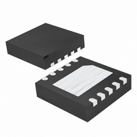
DS2746G+ Maxim Integrated Products, DS2746G+ Datasheet - Page 13

DS2746G+
Manufacturer Part Number
DS2746G+
Description
IC MON BATTERY 2-WIRE 10-TDFN
Manufacturer
Maxim Integrated Products
Datasheet
1.DS2746GTR.pdf
(17 pages)
Specifications of DS2746G+
Function
Fuel, Gas Gauge/Monitor
Battery Type
Lithium-Ion (Li-Ion); Nickel-Metal Hydride (NiMH)
Voltage - Supply
2.5 V ~ 5.5 V
Operating Temperature
-40°C ~ 85°C
Mounting Type
Surface Mount
Package / Case
10-WFDFN Exposed Pad
Operating Supply Voltage
2.5 V to 5.5 V
Maximum Operating Temperature
+ 85 C
Minimum Operating Temperature
- 40 C
Charge Safety Timers
No
Mounting Style
SMD/SMT
Temperature Monitoring
No
Lead Free Status / RoHS Status
Lead free / RoHS Compliant
STATUS/CONFIG REGISTER
The Status/Config register is read/write with individual bits designated as read only. Bit values indicate status as
well as program or select device functionality.
Figure 12. Status/Config Register Format
X — Reserved.
PORF — The Power-On-Reset Flag is set to indicate initial power-up. PORF is not cleared internally. The user
must write this flag value to a 0 in order to use it to indicate subsequent power-up events. If PORF indicates a
power-on-reset, the ACR could be misaligned with the actual battery state of charge. The system can request a
charge to full in order to synchronize the ACR with the battery charge state. PORF is read/write-to-zero.
SMOD — SLEEP Mode Enable. A value of 1 allows the DS2746 to enter sleep mode when SCL AND SDA are low
for t
NBEN — Negative Blanking Enable. A value of 1 enables blanking of negative current values up to 25µV. A value
of 0 disables blanking of negative currents. The power-up default is NBEN = 1.
V
the AIN1 conversion ends. The power-up default is V
AIN1 – AIN1 Conversion Valid. This read only bit indicates that the V
occurred on the AIN1 pin. When using the V
the AIN1 bit is set, should the AIN1 register be read.
AIN0 – AIN0 Conversion Valid. This read only bit indicates that the V
occurred on the AIN0 pin. When using the V
the AIN0 bit is set, should the AIN0 register be read.
2-WIRE BUS SYSTEM
The 2-Wire bus system supports operation as a slave-only device in a single or multislave, and single or
multimaster system. The 2-wire interface consists of a serial data line (SDA) and serial clock line (SCL). SDA and
SCL provide bidirectional communication between the DS2746 slave device and a master device at speeds up to
400 kHz. The DS2746’s SDA pin operates bidirectionally, that is, when the DS2746 receives data, SDA operates
as an input, and when the DS2746 returns data, SDA operates as an open drain output, with the host system
providing a resistive pullup. The DS2746 always operates as a slave device, receiving and transmitting data under
the control of a master device. The master initiates all transactions on the bus and generates the SCL signal as
well as the START and STOP bits which begin and end each transaction.
Bit Transfer
One data bit is transferred during each SCL clock cycle, with the cycle defined by SCL transitioning low-to-high and
then high-to-low. The SDA logic level must remain stable during the high period of the SCL clock pulse. Any
change in SDA when SCL is high is interpreted as a START or STOP control signal.
ODIS
SLEEP
– V
. A value of 0 disables the transition to sleep mode. The power-up default is SMOD = 1.
OUT
Disable. When set to 0 this output is driven t
BIT 7
X
PORF
BIT 6
SMOD
BIT 5
ODIS
ODIS
bit, before reading the AIN1 registers, read the AIN1 bit. Only once
bit, before reading the AIN0 registers, read the AIN0 bit. Only once
NBEN
BIT 4
ADDRESS 01
ODIS
13 of 17
= 0, a value of 1 disables the V
PRE
VODIS
BIT 3
before the AIN0 conversion begins, and disabled after
OUT
OUT
BIT 2
output was enabled, and a conversion has
output was enabled, and a conversion has
X
BIT 1
AIN1
OUT
output.
BIT 0
AIN0


