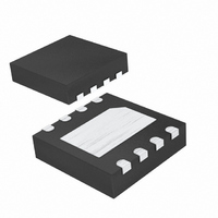
MAX16023PTAS12+T Maxim Integrated Products, MAX16023PTAS12+T Datasheet - Page 11

MAX16023PTAS12+T
Manufacturer Part Number
MAX16023PTAS12+T
Description
IC BATTERY BACKUP 1.2V 8TDFN-EP
Manufacturer
Maxim Integrated Products
Datasheet
1.MAX16023LTAL12T.pdf
(17 pages)
Specifications of MAX16023PTAS12+T
Function
Back-Up Management
Battery Type
All Battery Types
Voltage - Supply
1.53 V ~ 5.5 V
Operating Temperature
-40°C ~ 85°C
Mounting Type
Surface Mount
Package / Case
8-WDFN Exposed Pad
Lead Free Status / RoHS Status
Lead free / RoHS Compliant
The Typical Applications Circuit shows a typical con-
nection using the MAX16024. OUT powers the SRAM. If
V
lower than V
powered from V
regulator is in dropout, the regulator is powered from
BATT (see the Functional Diagrams ). OUT supplies up
to 100mA from V
In a brownout or power failure, it may be necessary to
preserve the contents of the RAM. With a backup-bat-
tery installed at BATT, the MAX16023/MAX16024 auto-
matically switch the RAM to backup power when V
falls. The MAX16024 has a BATT ON output that goes
high when in battery-backup mode. Three conditions
must be met for these devices to switch to battery
backup mode:
1) V
2) V
3) The regulator is in dropout (except for the 1.2V out-
Figure 1. Reset and Chip-Enable Timing
CC
put version).
CC
CC
is higher than the reset threshold (V
is lower than the reset threshold.
is lower than V
TH
RESET THRESHOLD V
CC
but higher than V
CC
______________________________________________________________________________________
. If V
.
Backup-Battery Switchover
BATT
Detailed Description
CC
CEOUT
RESET
CEIN
V
< V
.
CC
TH
TH
RESET-TO-CEOUT DELAY (12µs)
, V
BATT
CC
< V
, the regulator is
TH
BATT
), or if V
Battery-Backup Circuits with
, and the
t
RD
CC
CC
Regulated Output Voltage
is
The MAX16024 provides internal gating of CE signals to
prevent erroneous data from being written to CMOS
RAM in the event of a power failure or brownout. During
normal operation, the CE gate enables and passes all
CE transitions. When the reset output asserts, this path
becomes disabled, preventing erroneous data from cor-
rupting the CMOS RAM and CEOUT is pulled up to OUT
through an internal current source. The 1.5ns propaga-
tion delay from CEIN to CEOUT allows the devices to
be used with most µPs and high-speed DSPs.
During normal operation (reset not asserted), CEIN is
connected to CEOUT through a low on-resistance
transmission gate. If CEIN is high when a reset asserts,
CEOUT remains high regardless of any subsequent
transition on CEIN during the reset event.
If CEIN is low when reset asserts, CEOUT is held low for
12µs to allow completion of the read/write operation.
After the 12µs delay expires, CEOUT goes high and
stays high regardless of any subsequent transitions on
CEIN during the reset event. When CEOUT is discon-
nected from CEIN, CEOUT is actively pulled up to OUT.
The propagation delay through the chip-enable circuitry
depends on both the source impedance of the drive to
CEIN and the capacitive loading at CEOUT. Minimize
the capacitive load at CEOUT to minimize propagation
delay, and use a low-output-impedance driver.
Chip-Enable Signal Gating (MAX16024)
t
RP
t
RD
*
IF CEIN GOES HIGH BEFORE RESET ASSERTS,
CEOUT GOES HIGH WITHOUT DELAY AS
CEIN GOES HIGH.
*
t
RP
11


