MAX8903AETI+T Maxim Integrated Products, MAX8903AETI+T Datasheet - Page 22

MAX8903AETI+T
Manufacturer Part Number
MAX8903AETI+T
Description
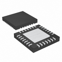
IC DC/DC CHARGER LI+ 28-TQFN
Manufacturer
Maxim Integrated Products
Series
Smart Power Selector™r
Datasheet
1.MAX8903AETI.pdf
(28 pages)
Specifications of MAX8903AETI+T
Function
Charge Management
Battery Type
Lithium-Ion (Li-Ion)
Voltage - Supply
4.1 V ~ 16 V
Operating Temperature
-40°C ~ 85°C
Mounting Type
Surface Mount
Package / Case
28-TQFN Exposed Pad
Lead Free Status / RoHS Status
Lead free / RoHS Compliant
2A 1-Cell Li+ DC-DC Chargers for USB
and Adapter Power
where:
R
ture T in Celsius
R
β = The material constant of the thermistor, which typi-
cally ranges from 3000K to 5000K
T = The temperature of the thermistor in °C
Table 3 shows the MAX8903A–MAX8903E/MAX8903Y
THM temperature limits for different thermistor material
constants.
Some designs might prefer other thermistor temperature
limits. Threshold adjustment can be accommodated by
changing R
parallel with the thermistor, or using a thermistor with dif-
ferent β. For example, a +45°C hot threshold and 0°C
cold threshold can be realized by using a thermistor
with a β of 4250 and connecting 120kΩ in parallel. Since
the thermistor resistance near 0°C is much higher than it
is near +50°C, a large parallel resistance lowers the
cold threshold, while only slightly lowering the hot
threshold. Conversely, a small series resistance raises
the hot threshold, while only slightly raising the cold
threshold. Raising R
thresholds, while lowering R
Note that since VL is active whenever valid input power
is connected at DC or USB, thermistor bias current
flows at all times, even when charging is disabled (CEN
= high). When using a 10kΩ thermistor and a 10kΩ
pullup to VL, this results in an additional 250μA load.
This load can be reduced to 25μA by instead using a
100kΩ thermistor and 100kΩ pullup resistor.
The power enabled on battery detection function allows
the MAX8903B/MAX8903E/MAX8903G to automatically
enable/disable the USB and DC power inputs when the
battery is applied/removed. This function utilizes the
battery pack’s integrated thermistor as a sensing mech-
anism to determine when the battery is applied or
removed. With this function, MAX8903B/MAX8903E/
MAX8903G-based systems shut down when the battery
is removed regardless of whether external power is
available at the USB or DC power inputs.
The MAX8903B/MAX8903E/MAX8903G implement the
power enabled on battery detection function with the
thermistor detector comparator as shown in Figure 7. If
no battery is present, the absence of the thermistor
allows R
THM pin increases above 87% of VL, it is assumed that
the battery has been removed and the system powers
down. However, there is also the option to bypass this
22
T
25
= The resistance in Ω of the thermistor at tempera-
= The resistance in Ω of the thermistor at +25°C
______________________________________________________________________________________
TB
TB
to pull THM to VL. When the voltage at the
, connecting a resistor in series and/or in
Power Enable on Battery Detection
TB
lowers both the cold and hot
TB
raises both thresholds.
thermistor sensing option completely, and so retain the
ability to remove the battery and let the system continue
to operate with external power. If the THM pin is tied to
GND (voltage at THM is below 3% of VL), the thermistor
option is disabled and the system does not respond to
the thermistor input. In those cases, it is assumed that
the system has its own temperature sensing, and halts
changing through CEN when the temperature is outside
of the safe charging range.
The MAX8903B/MAX8903E/MAX8903G have a SYS
load regulation of 25mV/A versus a load regulation of
40mV/A on the MAX8903A/MAX8903C/MAX8903D/
MAX8903Y. To achieve tighter load regulation, the loop
gain on the MAX8903B/MAX8903E/MAX8903G is high-
er. To ensure feedback loop stability with higher gain, a
larger SYS output capacitor is required (see Table 7).
The MAX8903 step-down DC-DC regulator implements
a control scheme that typically results in a 4MHz nomi-
nal switching frequency. When the input voltage
decreases to a value near the output voltage, high duty
cycle operation occurs and, due to minimum off-time
constraints, 4MHz operation is not achievable. The reg-
ulator then provides a fixed minimum off-time, peak cur-
rent regulation. Similarly, when the input voltage is too
high to allow 4MHz operation due to minimum on-time
constraints, the regulator becomes a fixed minimum on-
time valley current regulator.
For a given maximum output voltage, the minimum rip-
ple current condition occurs at the lowest input voltage
provided that the minimum input voltage allows the reg-
ulator to maintain 4MHz operation. If the minimum input
voltage dictates an off-time less than 100ns, then the
minimum ripple condition occurs just before the regula-
tor enters fixed minimum off-time operation. To allow
Table 4. Package Thermal Characteristics
Continuous
Power
Dissipation
θ
θ
JA
JC
28-PIN 4mm x 4mm THIN QFN
SINGLE-LAYER PCB
1666.7mW
Derate 20.8mW/°C
above +70°C
48°C/W
3°C/W
Minimum SYS Output Capacitor
Step-Down DC-DC Regulator
Inductor Selection for
Power Dissipation
MULTILAYER PCB
2286mW
Derate 28.6mW/°C
above +70°C
35°C/W
3°C/W


