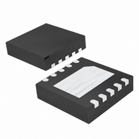
DS2746G+T&R Maxim Integrated Products, DS2746G+T&R Datasheet - Page 15

DS2746G+T&R
Manufacturer Part Number
DS2746G+T&R
Description
IC MON BATTERY 2-WIRE 10-TDFN
Manufacturer
Maxim Integrated Products
Datasheet
1.DS2746GTR.pdf
(17 pages)
Specifications of DS2746G+T&R
Function
Fuel, Gas Gauge/Monitor
Battery Type
Lithium-Ion (Li-Ion); Nickel-Metal Hydride (NiMH)
Voltage - Supply
2.5 V ~ 5.5 V
Operating Temperature
-40°C ~ 85°C
Mounting Type
Surface Mount
Package / Case
10-WFDFN Exposed Pad
Lead Free Status / RoHS Status
Lead free / RoHS Compliant
Table 5. 2-Wire Protocol Key
Basic Transaction Formats
Write:
A write transaction transfers one or more data bytes to the DS2746. The data transfer begins at the memory
address supplied in the MAddr byte. Control of the SDA signal is retained by the master throughout the transaction,
except for the Acknowledge cycles.
Read:
A read transaction transfers one or more bytes from the DS2746. Read transactions are composed of two parts, a
write portion followed by a read portion, and is therefore inherently longer than a write transaction. The write portion
communicates the starting point for the read operation. The read portion follows immediately, beginning with a
REPEATED START, Slave Address with R/W set to a 1. Control of SDA is assumed by the DS2746 beginning with
the Slave Address Acknowledge cycle. Control of the SDA signal is retained by the DS2746 throughout the
transaction, except for the Acknowledge cycles. The master indicates the end of a read transaction by responding
to the last byte it requires with a No Acknowledge. This signals the DS2746 that control of SDA is to remain with
the master following the Acknowledge clock.
Write Data Protocol
The write data protocol is used to write to register and shadow RAM data to the DS2746 starting at memory
address MAddr. Data0 represents the data written to MAddr, Data1 represents the data written to MAddr + 1 and
DataN represents the last data byte, written to MAddr + N. The master indicates the end of a write transaction by
sending a STOP or REPEATED START after receiving the last acknowledge bit.
The msb of the data to be stored at address MAddr can be written immediately after the MAddr byte is
acknowledged. Because the address is automatically incremented after the least significant bit (lsb) of each byte is
received by the DS2746, the msb of the data at address MAddr + 1 is can be written immediately after the
acknowledgement of the data at address MAddr. If the bus master continues an auto-incremented write transaction
beyond address 4Fh, the DS2746 ignores the data. Data is also ignored on writes to read-only addresses and
reserved addresses, locked EEPROM blocks as well as a write that auto increments to the Function Command
register (address FEh). Incomplete bytes and bytes that are Not Acknowledged by the DS2746 are not written to
memory. As noted in the Memory Section, writes to unlocked EEPROM blocks modify the shadow RAM only.
Read Data Protocol
The Read Data protocol is used to read register and shadow RAM data from the DS2746 starting at memory
address specified by MAddr. Data0 represents the data byte in memory location MAddr, Data1 represents the data
from MAddr + 1 and DataN represents the last byte read by the master.
S
SAddr
FCmd
MAddr
Data
A
N
KEY
S SAddr W A MAddr A Data0 A Data1 A … DataN A P
S SAddr W A MAddr A Sr SAddr R A Data0 A Data1 A … DataN N P
S SAddr W A MAddr A Data0 A P
S SAddr W A MAddr A Sr SAddr R A Data0 N P
START bit
Slave Address (7-bit)
Function Command byte
Memory Address byte
Data byte written by master
Acknowledge bit - Master
No Acknowledge - Master
Write Portion
DESCRIPTION
Read Portion
Sr
W
R
P
Data
A
N
KEY
15 of 17
Repeated START
R/W bit = 0
R/W bit = 1
STOP bit
Data byte returned by slave
Acknowledge bit - Slave
No Acknowledge - Slave
DESCRIPTION


