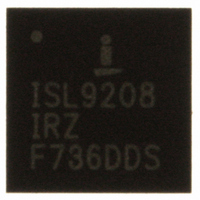
ISL9208IRZ Intersil, ISL9208IRZ Datasheet - Page 8

ISL9208IRZ
Manufacturer Part Number
ISL9208IRZ
Description
IC MULTI-CELL LI-ION PROT 32-QFN
Manufacturer
Intersil
Specifications of ISL9208IRZ
Function
Battery Monitor
Battery Type
Lithium-Ion (Li-Ion)
Voltage - Supply
5 V ~ 10 V
Operating Temperature
-40°C ~ 85°C
Mounting Type
Surface Mount
Package / Case
32-VQFN Exposed Pad, 32-HVQFN, 32-SQFN, 32-DHVQFN
Interface Type
I2C, Serial
Battery Protection
Over Current
No. Of Batteries
7
Supply Voltage Range
9.2V To 30.1V
Battery Ic Case Style
QFN
No. Of Pins
32
Rohs Compliant
Yes
Operating Temperature Range
-40°C To +85°C
Ic Interface Type
I2C
Lead Free Status / RoHS Status
Lead free / RoHS Compliant
Available stocks
Company
Part Number
Manufacturer
Quantity
Price
Company:
Part Number:
ISL9208IRZ
Manufacturer:
Intersil
Quantity:
500
Part Number:
ISL9208IRZ
Manufacturer:
INTERSIL
Quantity:
20 000
Company:
Part Number:
ISL9208IRZ-T
Manufacturer:
OSRAM
Quantity:
2 506
Operating Specifications
NOTES:
SERIAL INTERFACE CHARACTERISTICS
SCL Clock Frequency
Pulse Width Suppression Time at
SDA and SCL Inputs
SCL Falling Edge to SDA Output Data
Valid
Time the Bus Must Be Free Before
Start of New Transmission
Clock Low Time
Clock High Time
Start Condition Setup Time
Start Condition Hold Time
Input Data Setup Time
Input Data Hold Time
Stop Condition Setup Time
Stop Condition Hold Time
Data Output Hold Time
SDA and SCL Rise Time
SDA and SCL Fall Time
Capacitive Loading Of SDA Or SCL
SDA and SCL Bus Pull-up Resistor-
Off Chip
Input Leakage Current (SCL, SDA)
Input Buffer Low Voltage (SCL, SDA)
Input Buffer High Voltage (SCL, SDA)
Output Buffer Low Voltage (SDA)
SDA and SCL Input Buffer Hysteresis I
3. Power up of the device requires all V
4. The device provides an internal hold time of at least 300ns for the SDA signal to bridge the unidentified region of the falling edge of SCL.
5. Typical +125°C ±10%, based on design and characterization data.
6. Typical 5Ω ±2Ω, based on design and characterization data.
7. Maximum output capacitance = 15pF.
PARAMETER
8
Over the recommended operating conditions unless otherwise specified. (Continued)
SYMBOL
t
t
t
t
t
2
t
SU:STO
HD:STO
CELL1
SU:STA
HD:STA
SU:DAT
HD:DAT
R
CHYST Sleep bit = 0
t
t
f
t
HIGH
V
LOW
t
V
SCL
t
BUF
Cb
V
t
OUT
DH
I
AA
t
t
IN
OL
LI
R
F
IH
IL
, V
CELL2
Any pulse narrower than the max spec is
suppressed.
From SCL falling crossing V
SDA exits the V
window.
SDA crossing V
condition to SDA crossing V
the following START condition.
Measured at the V
Measured at the V
SCL rising edge to SDA falling edge. Both
crossing the V
From SDA falling edge crossing V
to SCL falling edge crossing V
From SDA exiting the V
window to SCL rising edge crossing
V
From SCL falling edge crossing V
SDA entering the V
window.
From SCL rising edge crossing V
SDA rising edge crossing V
From SDA rising edge to SCL falling edge.
Both crossing V
From SCL falling edge crossing V
until SDA enters the V
window. (Note 4)
From V
From V
Total on-chip and off-chip
Maximum is determined by t
For C
For C
Voltage relative to V
Voltage relative to V
I
OL
IL
(min).
= 1mA
, V
B
B
IL
IH
= 400pF, max is about 2kΩ ~ 2.5kΩ
= 40pF, max is about 15kΩ to 20kΩ
CELL3
(max) to V
(min) to V
TEST CONDITION
, and VCC to be above the limits specified.
IH
IL
ISL9208
IH
IH
(min) level.
(max) to V
(min) during a STOP
(min).
IL
IH
IL
IL
IH
SS
SS
(max) crossing.
(min) crossing.
(max).
(max) to V
(min).
IL
IL
of the device.
of the device.
(max) to V
(max) to V
IL
IH
IH
IH
R
(max).
(min), until
(min)
(min) during
IH
and t
IH
(min).
IH
IH
(min)
IL
IL
IH
(min) to
(min) to
IH
(max)
F
(max)
(min)
.
(min)
0.05 * V
V
RGO
MIN
250
300
-0.3
4.7
4.7
4.0
4.7
4.0
4.0
4.0
-10
0
1
x 0.7
RGO
TYP
V
V
RGO
RGO
MAX
1000
400
100
300
3.5
0.4
50
10
V
November 2, 2007
x 0.3
+ 0.1
FN6446.1
UNIT
kHz
kΩ
pF
µA
ns
µs
µs
µs
µs
µs
µs
ns
µs
µs
µs
ns
ns
ns
V
V
V
V


