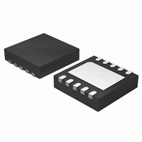
ISL9301IRZ-T Intersil, ISL9301IRZ-T Datasheet - Page 9

ISL9301IRZ-T
Manufacturer Part Number
ISL9301IRZ-T
Description
IC CHRGR LI-ION HV SGL 10-TDFN
Manufacturer
Intersil
Type
Battery Chargerr
Datasheet
1.ISL9301IRZ.pdf
(12 pages)
Specifications of ISL9301IRZ-T
Function
Charge Management
Battery Type
Lithium-Ion (Li-Ion), Lithium-Polymer (Li-Pol)
Voltage - Supply
4.3 V ~ 10 V
Operating Temperature
-40°C ~ 85°C
Mounting Type
Surface Mount
Package / Case
10-VFDFN Exposed Pad
Output Voltage
4.5V
Operating Supply Voltage (min)
4.3V
Operating Temp Range
-40C to 85C
Mounting
Surface Mount
Pin Count
10
Operating Temperature Classification
Industrial
Lead Free Status / RoHS Status
Lead free / RoHS Compliant
Applications Information
Input Bypass Capacitor
The input capacitor is required to suppress the power supply
transient response during transitions. Typically, a 10µF or
larger capacitor should be sufficient to suppress the power
supply noise.
Due to the inductance of the power leads of the wall adapter
or USB source, the input capacitor type must be properly
selected to prevent high voltage transient during a hot-plug
event. A tantalum capacitor is a good choice for its high
ESR, providing damping to the voltage transient. Multi-layer
ceramic capacitors, however, have a very low ESR and
hence when chosen as input capacitor, a 1Ω series resistor
must be used (as shown in the “Typical Application Circuit”
on page 6) to provide adequate damping.
FIGURE 5. CHARGE CURRENT FOLDBACK
VIN
X3
9
TEMPERATURE
MONITORING
+115°C
FIGURE 4. CHARGE CURRENT THERMAL FOLDBACK CIRCUIT
Q1
I
R
TEMPERATURE
I
I
T
R
I SEN
-40mA/°C
I
T
IREF
CONTROL
I
REF
SEN
ISL9301
+
-
CA
IREF
VOUT and VBAT Capacitor Selection
The criteria for selecting the capacitor at the VOUT and
VBAT pins is to maintain the stability as well as to bypass
any transient load current. The recommended capacitance is
a 4.7µF X5R ceramic capacitor for VOUT and 1µF for VBAT.
The actual capacitance connected to the output is
dependent on the actual application requirement.
Layout Guidance
The ISL9301 uses a thermally-enhanced DFN package that
has an exposed thermal pad at the bottom side of the
package. The layout should connect as much as possible to
copper on the exposed pad. Typically, the component layer
is more effective in dissipating heat. The thermal impedance
can be further reduced by using other layers of copper
connecting to the exposed pad through a thermal via array.
Each thermal via is recommended to have 0.3mm diameter
and 1mm distance from other thermal vias.
Input Power Sources
The input power source is typically a well-regulated wall
cube with 1m length wire or a USB port. The input voltage
ranges from 4.3V to 10V. The ISL9301 can withstand up to
28V on the input without damaging the IC. If the input
voltage is higher than the OVP threshold, the IC is disabled.
State Diagram
The state diagram is shown in Figure 6. There are 8 states to
cover all the operation modes, including the Trickle Charge,
Batt Discharge, PPM, CV Charge, Charge Fault, Charge
Complete, Disabled and OTP states.
The IC starts with a trickle charge or constant current charge
state depending on V
Trickle Charge state, the PPR is LO and the CHG is LO,
Q2
VA
+
-
BAT
VREF
when input power is applied. In the
X3
X3
VOUT
VBAT
July 2, 2008
FN6435.2


