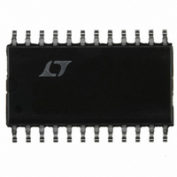
LT1511ISW Linear Technology, LT1511ISW Datasheet - Page 14

LT1511ISW
Manufacturer Part Number
LT1511ISW
Description
IC BATT CHRGR CONST I/V 3A24SOIC
Manufacturer
Linear Technology
Datasheet
1.LT1511CSWPBF.pdf
(16 pages)
Specifications of LT1511ISW
Function
Charge Management
Battery Type
Li-Ion, NiCd, NiMH
Voltage - Supply
6 V ~ 28 V
Operating Temperature
-40°C ~ 85°C
Mounting Type
Surface Mount
Package / Case
24-SOIC (0.300", 7.50mm Width)
Lead Free Status / RoHS Status
Contains lead / RoHS non-compliant
Available stocks
Company
Part Number
Manufacturer
Quantity
Price
Part Number:
LT1511ISW
Manufacturer:
LINEAR/凌特
Quantity:
20 000
Company:
Part Number:
LT1511ISW#PBF
Manufacturer:
TI
Quantity:
696
Part Number:
LT1511ISW#PBF
Manufacturer:
LINEAR/凌特
Quantity:
20 000
Company:
Part Number:
LT1511ISW#TRPBF
Manufacturer:
LT
Quantity:
3 140
Part Number:
LT1511ISW#TRPBF
Manufacturer:
LTNEAR
Quantity:
20 000
APPLICATIONS
LT1511
low thermal resistance system and to act as a ground
plane for reduced EMI.
Glue-on, chip-mounted heat sinks are effective only in
moderate power applications where the PC board copper
cannot be used, or where the board size is small. They
offer very little improvement in a properly laid out multi-
layer board of reasonable size.
Higher Duty Cycle for the LT1511 Battery Charger
Maximum duty cycle for the LT1511 is typically 90%, but
this may be too low for some applications. For example, if
an 18V 3% adapter is used to charge ten NiMH cells, the
charger must put out 15V maximum. A total of 1.6V is lost
in the input diode, switch resistance, inductor resistance
and parasitics, so the required duty cycle is 15/16.4 =
91.4%. As it turn out, duty cycle can be extended to 93%
14
110
100
Figure 8. LT1511 Thermal Resistance
90
80
70
60
50
40
45
40
35
30
25
20
15
10
Figure 9. LT1511 Lead Temperature
0
0
V
V
I
T
NOTE: PEAK DIE TEMPERATURE WILL BE
ABOUT 10 C HIGHER THAN LEAD TEMPER-
ATURE AT 3A CHARGING CURRENT
CHRG
A
MEASURED FROM AIR AMBIENT
TO DIE USING COPPER LANDS
AS SHOWN ON DATA SHEET
IN
BAT
= 25 C
= 16V
5
5
= 8.4V
= 3A
10
U
10
BOARD AREA (IN
BOARD AREA (IN
15
15
WITH V
INFORMATION
2-LAYER BOARD
4-LAYER BOARD
4-LAYER BOARD
2-LAYER BOARD
4-LAYER BOARD
U
20
20
BOOST
2
2
25
25
)
)
= 3.3V
W
30
30
LT1511 • F09
LT1511 • F08
35
35
U
0.47 F
STANDARD CONNECTION
C3
D2
V
Q1 = Si4435DY
Q2 = TP0610L
IN
by restricting boost voltage to 5V instead of using V
is normally done. This lower boost voltage also reduces
power dissipation in the LT1511, so it is a win-win deci-
sion. Connect an external source of 3V to 6V at V
Figure 10 with a 10 F C
Even Lower Dropout
For even lower dropout and/or reducing heat on the board,
the input diode D3 should be replaced with a FET (see
Figure 11). It is pretty straightforward to connect a
P-channel FET across the input diode and connect its gate
to the battery so that the FET commutates off when the
input goes low. The problem is that the gate must be
pumped low so that the FET is fully turned on even when
the input is only a volt or two above the battery voltage.
Also there is a turn-off speed issue. The FET should turn
SW
BOOST
SPIN
SENSE
LT1511
R
50k
X
Q1
Figure 11. Replacing the Input Diode
+
Figure 10. High Duty Cycle
BAT
HIGH DUTY CYCLE CONNECTION
D1
Q2
V
3V TO 6V
3V TO 6V
BAT
X
V
V
0.47 F
0.47 F
X
X
HIGH DUTY CYCLE CONNECTION
10 F
bypass capacitor.
10 F
C
C2
C
C3
D2
D2
X
X
+
SW
BOOST
SPIN
SENSE
SW
BOOST
SPIN
SENSE
LT1511
LT1511
V
CC
+
+
BAT
BAT
X
node in
BAT
1511 F11
1511 F10
V
V
BAT
BAT
as


