LTC6802IG-1#PBF Linear Technology, LTC6802IG-1#PBF Datasheet - Page 4
LTC6802IG-1#PBF
Manufacturer Part Number
LTC6802IG-1#PBF
Description
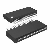
IC MONITOR BATT STACK MC 44-SSOP
Manufacturer
Linear Technology
Datasheet
1.LTC6802IG-1PBF.pdf
(38 pages)
Specifications of LTC6802IG-1#PBF
Function
Battery Monitor
Battery Type
Lithium-Ion (Li-Ion)
Voltage - Supply
4 V ~ 50 V
Operating Temperature
-40°C ~ 85°C
Mounting Type
Surface Mount
Package / Case
44-SOP (0.200", 5.30mm Width)
Lead Free Status / RoHS Status
Lead free / RoHS Compliant
Available stocks
Company
Part Number
Manufacturer
Quantity
Price


ELECTRICAL CHARACTERISTICS
LTC6802-1
temperature range, otherwise specifications are at T
SYMBOL PARAMETER
Voltage Mode Timing Specifications
t
t
t
t
t
t
t
t
t
Timing Specifications
t
t
t
t
Voltage Mode Digital I/O Specifications
V
V
V
Current Mode Digital I/O Specifications
I
I
I
I
I
I
I
I
Note 1: Stresses beyond those listed under Absolute Maximum Ratings
may cause permanent damage to the device. Exposure to any Absolute
Maximum Rating condition for extended periods may affect device
reliability and lifetime.
Note 2: The ADC specifications are guaranteed by the Total Measurement
Error (V
4
CYCLE
1
2
3
4
5
6
7
8
PD1
PD2
PD3
PD4
IH1
IL1
IH2
IL2
OH1
OL1
OH2
OL2
IH
IL
OL
ERR
) specification.
Discharge Switch On-Resistance
Temperature Range
Thermal Shutdown Temperature
Thermal Shutdown Hysteresis
Measurement Cycle Time
SDI Valid to SCKI Rising Setup
SDI Valid to SCKI Rising Hold
SCKI Low
SCKI High
CSBI Pulse Width
SCKI Rising to CSBI Rising
CSBI Falling to SCKI Rising
SCKI Falling to SDO Valid
Clock Frequency
Watchdog Timer Time Out Period
CSBI to CSBO
SCKI to SCKO
SDI to SDOI Write Delay
SDOI to SDI Read Delay
Digital Input Voltage High
Digital Input Voltage Low
Digital Output Voltage Low
Digital Input Current High
Digital Input Current Low
Digital Input Current High
Digital Input Current Low
Digital Output Current High
Digital Output Current Low
Digital Output Current High
Digital Output Current Low
CONDITIONS
V
Time Required to Measure 11 or 12 Cells
Time Required to Measure Up to 10 Cells
Time Required to Measure 1 Cell
C
C
C
C
Pins SCKI, SDI, and CSBI
Pins SCKI, SDI, and CSBI
Pin SDO; Sinking 500μA
Pins CSBI, SCKI, and SDI (Write)
Pins CSBI, SCKI, and SDI (Write)
Pin SDOI (Read)
Pin SDOI (Read)
Pins CSBO, SCKO, and SDOI (Write)
Pins CSBO, SCKO, and SDOI (Write)
Pin SDI (Read)
Pin SDI (Read)
CELL
CSBO
SCKO
SDOI
SDO
A
= 150pF
= 25°C. V
> 3V (Note 3)
= 150pF
= 150pF
= 150pF
The
l
+
denotes the specifications which apply over the full operating
= 43.2V, V
Note 3: Due to the contact resistance of the production tester, this
specification is tested to relaxed limits. The 20Ω limit is guaranteed by
design.
Note 4: V
combinations: Cn to Cn-1 for n = 2 to 12, C1 to V
voltage applied from V
Note 5: These absolute maximum ratings apply provided that the voltage
between inputs do not exceed their absolute maximum ratings.
–
= 0V, unless otherwise noted.
CELL
refers to the voltage applied across the following pin
TEMP1
or V
l
l
l
l
l
l
l
l
l
l
l
l
l
l
l
l
l
l
l
l
l
l
l
l
l
l
l
l
l
TEMP2
–1650
1000
1000
MIN
–40
250
400
400
400
100
100
–10
–10
9.2
11
10
1
1
2
to V
–
.
–1200
1200
TYP
145
1.2
10
13
11
–3
5
3
–
. V
TEMP
–1000
–1000
MAX
1650
13.5
250
600
300
300
300
1.5
2.5
0.8
0.3
20
85
16
10
10
refers to the
1
0
UNITS
68021fa
MHz
ms
ms
ms
μA
μA
μA
μA
μA
μA
μA
μA
°C
°C
°C
ns
ns
ns
ns
ns
ns
ns
ns
ns
ns
ns
ns
Ω
V
V
V
s
Related parts for LTC6802IG-1#PBF
Image
Part Number
Description
Manufacturer
Datasheet
Request
R

Part Number:
Description:
Manufacturer:
Linear Technology Corporation
Datasheet:

Part Number:
Description:
Multicell Addressable Battery Stack Monitor
Manufacturer:
LINER [Linear Technology]
Datasheet:

Part Number:
Description:
IC MONITOR BATT STACK 44-SSOP
Manufacturer:
Linear Technology
Datasheet:
Part Number:
Description:
IC MONITOR BATT STACK MC 44-SSOP
Manufacturer:
Linear Technology
Datasheet:
Part Number:
Description:
IC MONITOR BATT STACK 44-SSOP
Manufacturer:
Linear Technology
Datasheet:

Part Number:
Description:
CD ROM LINEARVIEW DATASHEETS
Manufacturer:
Linear Technology
Part Number:
Description:
Standalone Linear Li-Ion Battery Charger with Thermal Regulation in ThinSOT
Manufacturer:
Linear Technology Corporation
Datasheet:
Part Number:
Description:
Low noise, high frequency, 8th order linear phase lowpass filter
Manufacturer:
Linear Technology Corporation
Datasheet:
Part Number:
Description:
Manufacturer:
Linear Technology Corporation
Datasheet:
Part Number:
Description:
Manufacturer:
Linear Technology Corporation
Datasheet:
Part Number:
Description:
Manufacturer:
Linear Technology Corporation
Datasheet:
Part Number:
Description:
Manufacturer:
Linear Technology Corporation
Datasheet:
Part Number:
Description:
Manufacturer:
Linear Technology Corporation
Datasheet:
Part Number:
Description:
Manufacturer:
Linear Technology Corporation
Datasheet:
Part Number:
Description:
Manufacturer:
Linear Technology Corporation
Datasheet: