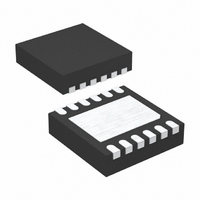
LT3650EDD-8.2#PBF Linear Technology, LT3650EDD-8.2#PBF Datasheet - Page 11

LT3650EDD-8.2#PBF
Manufacturer Part Number
LT3650EDD-8.2#PBF
Description
IC PWR MANAGER/CHRGR 12-DFN
Manufacturer
Linear Technology
Datasheet
1.LT3650EDD-8.4PBF.pdf
(20 pages)
Specifications of LT3650EDD-8.2#PBF
Function
Charge Management
Battery Type
Lithium-Ion (Li-Ion), Lithium-Polymer (Li-Pol)
Voltage - Supply
9 V ~ 32 V
Operating Temperature
-40°C ~ 85°C
Mounting Type
Surface Mount
Package / Case
12-WFDFN Exposed Pad
Input Voltage
32V
No. Of Outputs
1
Supply Voltage Range
9V To 32V
No. Of Pins
12
Operating Temperature Range
-40°C To +85°C
Msl
MSL 1 - Unlimited
Termination Type
SMD
Supply Voltage Min
9V
Rohs Compliant
Yes
Filter Terminals
SMD
Frequency
1MHz
Lead Free Status / RoHS Status
Lead free / RoHS Compliant
Available stocks
Company
Part Number
Manufacturer
Quantity
Price
APPLICATIONS INFORMATION
V
The LT3650 is biased directly from the charger input
supply through the V
switched currents, so a high quality, low ESR decoupling
capacitor is recommended to minimize voltage glitches
on V
input switching ripple current in the charger, so it must
have an adequate ripple current rating. RMS ripple current
(I
which has a maximum at V
The simple worst-case of 1/2 • I
used for design.
Bulk capacitance is a function of desired input ripple volt-
age (ΔV
10μF is typically adequate for most charger applications.
BOOST Supply
The BOOST bootstrapped supply rail drives the internal
switch and facilitates saturation of switch transistor. Oper-
ating range of the BOOST pin is 0V to 8.5V, as referenced
to the SW pin. Connect a 1μF or greater capacitor from
the BOOST pin to the SW pin.
The voltage on the decoupling capacitor is refreshed
through a diode, with the anode connected to/from either
the battery output voltage or an external source, and the
cathode connected to the BOOST pin. Rate the diode av-
erage current greater than 0.1A, and its reverse voltages
greater than V
IN
CVIN(RMS)
I
I
C
CVIN(RMS)
CVIN RMS
Input Supply
IN BULK
IN
(
. The V
(
IN
), and follows the relation:
) is:
)
)
= I
=
~
IN
IN(MAX)
I
I
CHG(MAX)
CHG MAX
MAX
decoupling capacitor (C
(
•
.
IN
⎛
⎝ ⎜
V
)
pin. This supply provides large
/2
BAT
•
Δ
IN
⎛
⎜
⎝
V
V
V
BAT
/
IN
= 2 • V
IN
V
IN
CHG(MAX)
⎞
⎟
⎠
⎞
⎠ ⎟
•
(
BAT
⎛
⎜
⎝
μ
⎡
⎢
⎣ ⎣
F
V
, where:
)
VIN
V
BAT
IN
is commonly
) absorbs all
⎤
⎥ −
⎦
⎟ 1
⎞
⎠
2
1
V
The LT3650 operates with a V
a start-up voltage requirement exists due to the nature of
the nonsynchronous step-down switcher topology used
for the charger. If there is no BOOST supply available,
the internal switch requires (V
This requirement does not exist if the BOOST supply is
available and (V
When an LT3650 charger is not switching, the SW pin is at
the same potential as the battery, which can be as high as
V
least 3V above the SW pin. The minimum start-up speci-
fi cation of V
to satisfy this requirement. Once switching begins, the
BOOST supply capacitor gets charged such that (V
– V
In low V
by an external source for start-up, eliminating the V
start-up requirement.
V
An LT3650 charger output requires bypass capacitance
connected from the BAT pin to ground (C
ramic capacitor is required for all applications. In systems
where the battery can be disconnected from the charger
output, additional bypass capacitance may be desired for
visual indication of a no-battery condition (see the Status
Pins section).
If it is desired to operate a system load from the LT3650
charger output when the battery is disconnected, additional
bypass capacitance is required. In this type of application
with the charger being used as a DC/DC converter, exces-
sive ripple and/or low amplitude oscillations can occur
without additional output bulk capacitance. For these ap-
plications, place a 100μF low ESR nonceramic capacitor
(chip tantalum or organic semiconductor capacitors such
as Sanyo OS-CONs or POSCAPs) from BAT to ground,
in parallel with the 10μF ceramic bypass capacitor. This
additional bypass capacitance may also be required in
systems where the battery is connected to the charger
through long wires. The voltage rating on C
or exceed the battery fl oat voltage.
IN
BAT(FLT)
BAT
SW
/ BOOST Start-Up Requirement
Output Decoupling
) > 2V, and the V
IN
. For reliable start-up, the V
applications, the BOOST supply can be powered
IN
LT3650-8.2/LT3650-8.4
at or above 11.5V provides ample margin
BOOST
– V
IN
requirement no longer applies.
SW
IN
) > 2V.
range of 9V to 32V, however,
IN
– V
SW
IN
supply must be at
) > 3V to operate.
BAT
BAT
). A 10μF ce-
must meet
11
36508284fc
BOOST
IN


