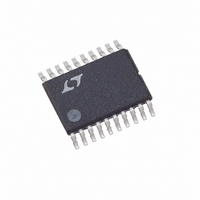
LTC4011CFE#TRPBF Linear Technology, LTC4011CFE#TRPBF Datasheet - Page 22

LTC4011CFE#TRPBF
Manufacturer Part Number
LTC4011CFE#TRPBF
Description
IC BATT CHARGER HIEFF 20TSSOP
Manufacturer
Linear Technology
Datasheet
1.LTC4011CFEPBF.pdf
(26 pages)
Specifications of LTC4011CFE#TRPBF
Function
Charge Management
Battery Type
Nickel Cadmium (NiCd), Nickel Metal-Hydride (NiMH)
Voltage - Supply
4.5 V ~ 34 V
Operating Temperature
0°C ~ 85°C
Mounting Type
Surface Mount
Package / Case
20-TSSOP (0.173", 4.40mm Width) Exposed Pad
Lead Free Status / RoHS Status
Lead free / RoHS Compliant
Available stocks
Company
Part Number
Manufacturer
Quantity
Price
LTC4011
applicaTions inForMaTion
A second possibility is to configure an LTC4011-based
charger to accept battery packs with varying numbers of
cells. By including R2 of the average cell voltage divider
network shown in Figure 3, battery-based programming
of the number of series-stacked cells could be realized
without defeating LTC4011 detection of battery insertion
or removal. Figure 12 shows a 2-cell NiMH battery pack
that programs the correct number of series cells when it is
connected to the charger, along with indicating chemistry
and providing temperature information.
Any of these battery pack charge control concepts could be
combined in a variety of ways to service custom application
needs. Charging parallel cells is not recommended.
Figure 11. NiCd Battery Pack with Time Limit Control
TIMER
10
66.5k
(PAUSE)
READY
CHEM
CHRG
NC
4
TOC
V
TEMP
7
10k
NTC
+
–
1200mAhr
NiCd CELLS
BATTERY
PACK
4011 F11
Figure 10. Charging Waveforms Example
PCB Layout Considerations
To prevent magnetic and electrical field radiation and
high frequency resonant problems, proper layout of the
components connected to the LTC4011 is essential. Refer
to Figure 13. For maximum efficiency, the switch node
rise and fall times should be minimized. The following
PCB design priority list will help ensure proper topology.
Layout the PCB using this specific order.
1. Input capacitors should be placed as close as possible
Figure 12. NiMH Battery Pack Indicating Number of Cells
to switching FET supply and ground connections with
the shortest copper traces possible. The switching
FETs must be on the same layer of copper as the input
CHEM
4
V
TEMP
7
10k
NTC
V
CELL
8
R2
+
–
1500mAhr
NiMH CELLS
BATTERY
PACK
4011 F12
4011fb


