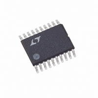
LTC4011CFE#TR Linear Technology, LTC4011CFE#TR Datasheet - Page 4

LTC4011CFE#TR
Manufacturer Part Number
LTC4011CFE#TR
Description
IC BATT CHARGER HIEFF 20TSSOP
Manufacturer
Linear Technology
Datasheet
1.LTC4011CFEPBF.pdf
(26 pages)
Specifications of LTC4011CFE#TR
Function
Charge Management
Battery Type
Nickel Cadmium (NiCd), Nickel Metal-Hydride (NiMH)
Voltage - Supply
4.5 V ~ 34 V
Operating Temperature
0°C ~ 85°C
Mounting Type
Surface Mount
Package / Case
20-TSSOP (0.173", 4.40mm Width) Exposed Pad
Lead Free Status / RoHS Status
Contains lead / RoHS non-compliant
Available stocks
Company
Part Number
Manufacturer
Quantity
Price
LTC4011
elecTrical characTerisTics
SYMBOL
T
V
V
Charger Timing
∆t
∆t
PowerPath Control
V
V
V
t
Status and Chemistry Select
V
I
I
V
V
I
I
Note 1: Stresses beyond those listed under Absolute Maximum Ratings
may cause permanent damage to the device. Exposure to any Absolute
Maximum Rating condition for extended periods may affect device
reliability and lifetime.
Note 2: The LTC4011C is guaranteed to meet performance specifications
from 0°C to 70°C. Specifications over the 0°C to 85°C operating
temperature range are assured by design, characterization and correlation
with statistical process controls.
Note 3: Operating junction temperature T
the ambient temperature T
dissipation P
Refer to the Applications Information section for details. This IC includes
overtemperature protection that is intended to protect the device during
momentary overload conditions. Junction temperature will exceed 125°C
temperature range, otherwise specifications are at T
OFF(INFET)
LKG
IH(VCDIV)
IL
IH
MAXC
TEMP(D)
TEMP(P)
FR
OL(INFET)
OH(INFET)
OL
IL
IH
TIMER
MAX
T
J
= T
A
+ θ
D
PARAMETER
Maximum Fast Charge Temperature
(Note 8)
V
Pause Threshold Voltage
Internal Time Base Error
Programmable Timer Error
INFET Forward Regulation Voltage
Output Voltage Low
Output Voltage High
INFET OFF Delay Time
Output Voltage Low (I
Output Leakage Current
Input Current High
Input Voltage Low
Input Voltage High
Input Current Low
Input Current High
(in watts) by the formula:
JA
TEMP
• P
D
Disable Threshold Voltage
A
and the total continuous package power
LOAD
= 10mA)
J
(in °C) is calculated from
CONDITIONS
V
R
DCIN – V
V
V
C
V
All Other Status Outputs
All Status Outputs Inactive, V
V
CHEM (NiMH)
CHEM (NiCd)
CHEM = GND
CHEM = 3.3V
A
TEMP
CC
CC
LOAD
CDIV
CDIV
TIMER
= 25°C. V
– INFET, No Load
– INFET, No Load
= V
Decreasing, Fast Charge
= 10nF, INFET to 50%
= 49.9k
The
CC
BAT
l
(Shutdown)
CC
indicates specifications which apply over the full operating
= 12V, BAT = 4.8V, GND = PGND = 0V, unless otherwise noted.
when overtemperature protection is active. Continuous operation above
the specified maximum operating junction temperature may result in
device degradation or failure.
Note 4: All current into device pins is positive. All current out of device
pins is negative. All voltages are referenced to GND, unless otherwise
specified.
Note 5: These limits are guaranteed by correlation to wafer level
measurements.
Note 6: Output current may be limited by internal power dissipation. Refer
to the Applications Information section for details.
Note 7: Either TGATE V
Note 8: These limits apply specifically to the thermistor network shown in
Figure 5 in the Applications Information section with the values specified
for a 10k NTC (β of 3750). Limits are then guaranteed by specific V
voltage measurements during test.
OUT
= V
CC
l
l
l
l
l
l
l
l
l
l
l
l
l
l
l
l
OH
may apply for 7.5V < V
MIN
3.75
2.85
130
–10
–20
–10
–20
–20
2.8
57
15
–1
TYP
435
300
5.2
60
55
0
3
CC
< 9V.
MAX
280
100
700
600
900
3.3
63
10
20
50
15
10
–5
20
7
1
TEMP
UNITS
4011fb
mV
mV
mV
mV
mV
mV
µA
µA
µA
µA
°C
µs
%
%
V
V
V


