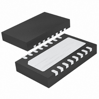
LTC3550EDHC#PBF Linear Technology, LTC3550EDHC#PBF Datasheet - Page 18

LTC3550EDHC#PBF
Manufacturer Part Number
LTC3550EDHC#PBF
Description
IC CHARGER BATT DUAL 16-DFN
Manufacturer
Linear Technology
Datasheet
1.LTC3550EDHCPBF.pdf
(24 pages)
Specifications of LTC3550EDHC#PBF
Function
Charge Management
Battery Type
Lithium-Ion (Li-Ion)
Voltage - Supply
4.3 V ~ 8 V
Operating Temperature
-40°C ~ 85°C
Mounting Type
Surface Mount
Package / Case
16-WFDFN Exposed Pad
Lead Free Status / RoHS Status
Lead free / RoHS Compliant
Available stocks
Company
Part Number
Manufacturer
Quantity
Price
LTC3550
APPLICATIO S I FOR ATIO
2. I
The R
be obtained from the Typical Performance Characteristics
curves. Thus, to obtain I
and multiply the result by the square of the average output
current. Other losses including C
tive losses and inductor core losses generally account for
less than 2% total additional loss.
Thermal Considerations
The battery charger’s thermal regulation feature and the
buck regulator’s high effi ciency make it unlikely that enough
power will be dissipated to exceed the LTC3550 maximum
junction temperature. Nevertheless, it is a good idea to
do some thermal analysis for worst-case conditions.
The junction temperature, T
where T
rise is given by:
where P
resistance from the junction of the die to the ambient
temperature.
18
internal switches, R
continuous mode, the average output current fl owing
through inductor L is “chopped” between the main
switch and the synchronous switch. Thus, the series
resistance looking into the SW pin is a function of both
top and bottom MOSFET R
(DC) as follows:
switch gate charge currents. The gate charge current
results from switching the gate capacitance of the
internal power MOSFET switches. Each time the gate
is switched from high to low to high again, a packet of
charge, dQ, moves from V
dQ/dt is the current out of V
than the DC bias current. In continuous mode, I
= f(Q
the internal top and bottom switches. Both the DC bias
and gate charge losses are proportional to V
thus their effects will be more pronounced at higher
supply voltages.
R
T
2
RISE
SW
R losses are calculated from the resistances of the
DS(ON)
T
= (R
A
D
= P
+ Q
is the power dissipated and θ
is the ambient temperature. The temperature
D
DS(ON)TOP
B
for both the top and bottom MOSFETs can
• θ
) where Q
JA
U
)(DC) + (R
SW
T
2
R losses, simply add R
, and external inductor R
and Q
U
J
, is given by: T
CC
DS(ON)
CC
B
to ground. The resulting
IN
DS(ON)BOT
are the gate charges of
and C
that is typically larger
W
and the duty cycle
OUT
JA
)(1 – DC)
is the thermal
J
ESR dissipa-
= T
U
A
SW
GATECHG
+ T
CC
to R
L
RISE
and
. In
L
In most applications the buck regulator does not dissi-
pate much heat due to its high effi ciency. The majority of
the LTC3550 power dissipation occurs when charging a
battery. Fortunately, the LTC3550 automatically reduces
the charge current during high power conditions using
a patented thermal regulation circuit. Thus, there is no
need to design for worst-case power dissipation scenarios
because the LTC3550 ensures that the battery charger
power dissipation never raises the junction temperature
above a preset value of 105°C. In the unlikely case that
the junction temperature is forced above 105°C (due to
abnormally high ambient temperatures or excessive buck
regulator power dissipation), the battery charge current will
be reduced to zero and thus dissipate no heat. As an added
measure of protection, even if the junction temperature
reaches approximately 150°C, the buck regulator’s power
switches will be turned off and the SW node will become
high impedance.
The conditions that cause the LTC3550 to reduce charge
current through thermal feedback can be approximated by
considering the power dissipated in the IC. The approxi-
mate ambient temperature at which the thermal feedback
begins to protect the IC is:
Most of the charger’s power dissipation is generated from
the internal charger MOSFET. Thus, the power dissipation
is calculated to be:
V
V
rent.
Example: An LTC3550 operating from a 5V wall adapter
(on the DCIN input) is programmed to supply 650mA
full-scale current to a discharged Li-Ion battery with a
voltage of 3V.
The charger power dissipation is calculated to be:
IN
BAT
T
T
T
P
P
A
A
A
is the charger supply voltage (either DCIN or USBIN),
D(CHARGER)
D(CHARGER)
= 105°C – T
= 105°C – (P
= 105°C – (P
is the battery voltage and I
= (V
= (5V – 3V) • 650mA = 1.3W
RISE
D
D(CHARGER)
IN
• θ
– V
JA
)
BAT
) • I
+ P
BAT
D(BUCK)
BAT
is the charge cur-
) • θ
JA
3550fa
(5)
(6)


