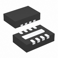
LTC4068EDD-4.2 Linear Technology, LTC4068EDD-4.2 Datasheet - Page 11

LTC4068EDD-4.2
Manufacturer Part Number
LTC4068EDD-4.2
Description
IC BATT CHARGER W/PROG TERM 8DFN
Manufacturer
Linear Technology
Datasheet
1.LTC4068EDD-4.2PBF.pdf
(12 pages)
Specifications of LTC4068EDD-4.2
Function
Charge Management
Battery Type
Lithium-Ion (Li-Ion)
Voltage - Supply
4.25 V ~ 6.5 V
Operating Temperature
-40°C ~ 85°C
Mounting Type
Surface Mount
Package / Case
8-WFDFN Exposed Pad
Lead Free Status / RoHS Status
Contains lead / RoHS non-compliant
Available stocks
Company
Part Number
Manufacturer
Quantity
Price
Company:
Part Number:
LTC4068EDD-4.2
Manufacturer:
LT
Quantity:
10 000
Part Number:
LTC4068EDD-4.2
Manufacturer:
LT
Quantity:
20 000
Company:
Part Number:
LTC4068EDD-4.2#PBF
Manufacturer:
ST
Quantity:
142
Company:
Part Number:
LTC4068EDD-4.2#TRPBF
Manufacturer:
ON
Quantity:
145
APPLICATIO S I FOR ATIO
PACKAGE DESCRIPTIO
Reverse Polarity Input Voltage Protection
In some applications, protection from reverse polarity
voltage on V
enough, a series blocking diode can be used. In other
cases, where the voltage drop must be kept low, a P-channel
MOSFET can be used (as shown in Figure 4).
CC
is desired. If the supply voltage is high
3.5 ±0.05
U
2.15 ±0.05
U
RECOMMENDED SOLDER PAD PITCH AND DIMENSIONS
TOP MARK
1.65 ±0.05
(2 SIDES)
Information furnished by Linear Technology Corporation is believed to be accurate and reliable.
However, no responsibility is assumed for its use. Linear Technology Corporation makes no represen-
tation that the interconnection of its circuits as described herein will not infringe on existing patent rights.
0.28 ± 0.05
PIN 1
0.200 REF
NOTE:
1. DRAWING TO BE MADE A JEDEC PACKAGE OUTLINE M0-229 VARIATION OF (WEED-1)
2. ALL DIMENSIONS ARE IN MILLIMETERS
3. DIMENSIONS OF EXPOSED PAD ON BOTTOM OF PACKAGE DO NOT INCLUDE
4. EXPOSED PAD SHALL BE SOLDER PLATED
W
MOLD FLASH. MOLD FLASH, IF PRESENT, SHALL NOT EXCEED 0.15mm ON ANY SIDE
U
2.38 ±0.05
(2 SIDES)
8-Lead Plastic DFN (3mm × 3mm)
(Reference LTC DWG # 05-08-1698)
U
0.50
BSC
DD Package
0.675 ±0.05
3.00 ±0.10
0.75 ±0.05
(4 SIDES)
PACKAGE
OUTLINE
0.00 – 0.05
Figure 4. Low Loss Input Reverse Polarity Protection
LTC4068-4.2/LTC4068X-4.2
1.65 ± 0.10
(2 SIDES)
V
BOTTOM VIEW—EXPOSED PAD
IN
0.28 ± 0.05
R = 0.115
DIODE OF FET
DRAIN-BULK
TYP
4
5
2.38 ±0.10
(2 SIDES)
8
1
0.50 BSC
V
CC
0.38 ± 0.10
LTC4068
(DD8) DFN 0203
405842 F04
11
406842fa


