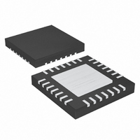
MAX8725ETI+ Maxim Integrated Products, MAX8725ETI+ Datasheet - Page 18

MAX8725ETI+
Manufacturer Part Number
MAX8725ETI+
Description
IC CHARGER BATTERY 28-TQFN
Manufacturer
Maxim Integrated Products
Datasheet
1.MAX1909ETI.pdf
(30 pages)
Specifications of MAX8725ETI+
Function
Charge Management
Battery Type
Multi-Chemistry
Voltage - Supply
8 V ~ 28 V
Operating Temperature
-40°C ~ 85°C
Mounting Type
Surface Mount
Package / Case
28-WFQFN Exposed Pad
Product
Charge Management
Operating Supply Voltage
8 V to 28 V
Supply Current
2.7 mA
Maximum Operating Temperature
+ 85 C
Minimum Operating Temperature
- 40 C
Charge Safety Timers
No
Mounting Style
SMD/SMT
Temperature Monitoring
No
Uvlo Start Threshold
9.18 V
Uvlo Stop Threshold
9.42 V
Lead Free Status / RoHS Status
Lead free / RoHS Compliant
Multichemistry Battery Chargers with Automatic
System Power Selector
The input range for ICTL is 0 to 3.6V on the MAX1909,
and 0 to 3.2V on the MAX8725. The charger shuts down
if ICTL is forced below 0.75V for the MAX1909 and 0.06V
for the MAX8725. When choosing current-sense resistor
RS2, note that it must have a sufficient power rating to
handle the full-load current. The sense resistor’s I
power loss reduces charger efficiency. Adjusting ICTL to
drop the voltage across the current-sense resistor
improves efficiency, but may degrade accuracy due to
the current-sense amplifier’s input offset error. The
charge-current error amplifier (GMI) is compensated at
the CCI pin. See the Compensation section.
The MAX1909 includes a battery voltage comparator
that allows a conditioning charge of overdischarged Li+
battery packs. If the battery-pack voltage is less than
3.1V x the number of cells programmed by MODE, the
MAX1909 charges the battery with 300mA current when
using sense resistor RS2 = 0.015Ω. After the battery
voltage exceeds the conditioning charge threshold, the
MAX1909 resumes full-charge mode, charging to the
programmed voltage and current limits. The MAX8725
does not provide automatic support for providing a
conditioning charge. To configure the MAX8725 to pro-
vide a conditioning charge current, ICTL should be
directly driven.
The total input current, from a wall cube or other DC
source, is the sum of the system supply current and the
current required by the charger. The MAX1909/MAX8725
reduce the source current by decreasing the charge cur-
rent when the input current exceeds the set input current
limit. This technique does not truly limit the input current.
As the system supply current rises, the available charge
current drops proportionally to zero. Thereafter, the total
input current can increase without limit.
An internal amplifier compares the differential voltage
between CSSP and CSSN to a scaled voltage set with
the CLS input. V
resistive voltage-divider between REF and GND.
Connect CLS to REF to set the input current-limit sense
voltage to the maximum value of 75mV. Calculate the
input current as follows:
V
error amplifier. Sense resistor RS1 sets the maximum
allowable source current. Once the input current limit is
reached, the charge current is decreased linearly until
the input current is below the desired threshold.
18
CLS
______________________________________________________________________________________
determines the reference voltage of the GMS
Setting the Input Current Limit
CLS
I
IN
can be driven directly or set with a
=
0 075
RS
.
1
Conditioning Charge
×
V
V
CLS
REF
2
R
Duty cycle affects the accuracy of the input current
limit. AC load current also affects accuracy (see the
Typical Operating Characteristics ). Refer to the
MAX1909/MAX8725 EV kit data sheet for more details
on reducing the effects of switching noise.
When choosing the current-sense resistor RS1, carefully
calculate its power rating. Take into account variations
in the system’s load current and the overall accuracy of
the sense amplifier. Note that the voltage drop across
RS1 contributes additional power loss, which reduces
efficiency.
System currents normally fluctuate as portions of the
system are powered up or put to sleep. Without input
current regulation, the input source must be able to
deliver the maximum system current and the maximum
charger input current. By using the input current-limit
circuit, the output current capability of the AC wall
adapter can be lowered, reducing system cost.
The MAX1909/MAX8725 include an input current monitor
IINP. The current delivered at the IINP output is a scaled-
down replica of the system load current plus the input-
referred charge current that is sensed across CSSP and
CSSN inputs. The output voltage range is 0 to 3V.
The voltage of IINP is proportional to the input current
according to the following equation:
where I
adapter power, G
(3mA/V typ), and R9 is the resistor connected between
IINP and ground.
Leave the IINP pin unconnected if not used.
LDO provides a 5.4V supply derived from DCIN and
can deliver up to 10mA of extra load current. The low-
side MOSFET driver is powered by DLOV, which must
be connected to LDO as shown in Figure 1. LDO also
supplies the 4.2235V reference (REF) and most of the
control circuitry. Bypass LDO with a 1µF capacitor.
When the AC adapter is removed, the MAX1909/
MAX8725 shut down to a low-power state that does not
significantly load the battery. Under these conditions, a
maximum of 6µA is drawn from the battery through the
combined load of the SRC, CSSP, CSSN, CSIP, CSIN,
and BATT inputs. The charger enters this low-power state
when DCIN falls below the undervoltage-lockout (UVLO)
threshold of 7V. The PDS switch turns off, the PDL switch
turns on, and the system runs from the battery.
Shutdown and Charge Inhibit ( PKPRES )
SOURCE
V
IINP
= I
is the DC current supplied by the AC
IINP
SOURCE
is the transconductance of IINP
✕
Current Measurement
R
S1
✕
G
IINP
LDO Regulator
✕
R
9


