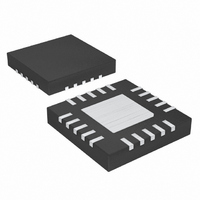
MAX17435ETG+ Maxim Integrated Products, MAX17435ETG+ Datasheet - Page 24

MAX17435ETG+
Manufacturer Part Number
MAX17435ETG+
Description
IC SMBUS BATT CHARGER 24TQFN
Manufacturer
Maxim Integrated Products
Datasheet
1.MAX17435ETG.pdf
(28 pages)
Specifications of MAX17435ETG+
Function
Charge Management
Battery Type
Multi-Chemistry
Voltage - Supply
8 V ~ 26 V
Operating Temperature
-40°C ~ 85°C
Mounting Type
Surface Mount
Package / Case
24-TQFN Exposed Pad
Product
Charge Management
Operating Supply Voltage
7 V to 26 V
Supply Current
1.5 mA
Maximum Operating Temperature
+ 85 C
Minimum Operating Temperature
- 40 C
Charge Safety Timers
Yes
Temperature Monitoring
Yes
Uvlo Stop Threshold
3.9 V
Lead Free Status / RoHS Status
Lead free / RoHS Compliant
High-Frequency,
Low-Cost SMBus Chargers
controller to initiate a new cycle. If the peak inductor
current exceeds IMAX comparator threshold or the output
voltage exceeds the OVP threshold, then the on-time is
terminated. The cycle-by-cycle current limit effectively
protects against overcurrent and short-circuit faults.
If, during the off-time, the inductor current goes to zero, the
ZCMP comparator output pulls high, turning off the low-side
MOSFET. Both the high- and low-side MOSFETs are turned
off until another cycle is ready to begin. The MAX17435/
MAX17535 enter into the discontinuous conduction mode
(see the Discontinuous Conduction section).
The on-time is calculated according to the following
equation:
where:
There is a 0.3Fs minimum off-time when the (V
V
x V
reached and the off-time is fixed at 0.27Fs. The switching
frequency in this mode varies according to the equation:
The
discontinuous conduction mode to ensure that the
inductor current is always positive. The MAX17435/
MAX17535 enter discontinuous conduction mode when
the output of the LVC control point falls below 110mV. For
RS2 = 10mI, this corresponds to 367mA:
where I
conduction.
In discontinuous mode, a new cycle is not started until
the LVC voltage rises above 150mV. Discontinuous
mode operation can occur during conditioning charge of
overdischarged battery packs, when the charge current
has been reduced sufficiently by the CCS control loop,
or when the charger is in constant-voltage mode with a
nearly full battery pack.
24
BATT
DCIN
_____________________________________________________________________________________
) differential becomes too small. If V
MAX17435/MAX17535
DIS
, then the threshold for minimum off-time is
is the current level for discontinuous
I
DIS
f
I
=
RIPPLE
t
ON
V
=
CSSN
L I
1
2
=
×
×
V
15 RS2
=
RIPPLE
110mV
CSSN
L I
- V
V
×
×
BATT
Discontinuous Conduction
BATT
1
RIPPLE
- V
can
L
×
=
BATT
+
t
367mA
OFF
t
OFF
also
BATT
operate
DCIN
R 0.88
in
-
Under extremely light loads, the BST capacitor may
become discharged if there is no DLO pulse. After 192µs
(typ), the MAX17435/MAX17535 turn on DLO for 300ns
and 550ns, respectively, to recharge the BST capacitor.
This DLO pulse need not be followed by a DHI pulse.
The CCI loop is internally compensated. The CCV and
the CCS share the external compensation capacitor.
The control loop, which is dominant, uses the external
compensation cap and the one that is not used uses an
internal compensation capacitor.
The simplified schematic in Figure 6 is sufficient to
describe the operation of the MAX17435/MAX17535
when the voltage loop (CCV) is in control. The required
compensation network is a pole-zero pair formed with
C
necessary to roll off the voltage loop’s response at low
frequency; C
The DHI and DLO outputs are optimized for driving
moderate-sized power MOSFETs. The MOSFET drive
capability is the same for both the low-side and high-
sides switches. This is consistent with the variable duty
factor that occurs in the notebook computer environment
where the battery voltage changes over a wide range.
There must be a low-resistance, low-inductance path
from the DLO driver to the MOSFET gate to prevent shoot-
through. Otherwise, the sense circuitry in the MAX17435/
MAX17535 interprets the MOSFET gate as off while there
is still charge left on the gate. Use very short, wide traces
measuring 10 squares to 20 squares or less (1.25mm to
2.5mm wide if the MOSFET is 25mm from the device).
Unlike the DLO output, the DHI output uses a 50ns (typ)
delay time to prevent the low-side MOSFET from turning
on until DHI is fully off. The same considerations should be
used for routing the DHI signal to the high-side MOSFET.
Figure 6. CC Loop Diagram
CC
and R
R
CC,
CC
C
CC
CC
CC
= 330pF is sufficient for most applications.
which is an internal 1.7kI. The pole is
R
OGMV
G
g
M(OUT)
MV
CCV Loop Compensation
REF
BATT
MOSFET Drivers
Compensation
R
C
ESR
OUT
R
L


