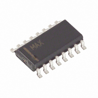
DS2715Z+ Maxim Integrated Products, DS2715Z+ Datasheet - Page 15

DS2715Z+
Manufacturer Part Number
DS2715Z+
Description
IC NIMH CHARGER 16-SOIC
Manufacturer
Maxim Integrated Products
Datasheet
1.DS2715Z.pdf
(17 pages)
Specifications of DS2715Z+
Function
Charge Management
Battery Type
Nickel Metal Hydride (NiMH)
Voltage - Supply
4.5 V ~ 16 V
Operating Temperature
-20°C ~ 85°C
Mounting Type
Surface Mount
Package / Case
16-SOIC (0.154", 3.90mm Width)
Operating Supply Voltage
16.5 V
Supply Current
1.3 mA
Maximum Operating Temperature
+ 85 C
Minimum Operating Temperature
- 20 C
Charge Safety Timers
Yes
Mounting Style
SMD/SMT
Temperature Monitoring
Yes
Uvlo Start Threshold
3.9 V
Uvlo Stop Threshold
35 mV
Lead Free Status / RoHS Status
Lead free / RoHS Compliant
DS2715: NiMH Battery Pack Charge Controller
Cell Stack Size Adjustment
R12 and R13 of the application circuits form a voltage divider such that the voltage of a single cell is present on the
Vbatt pin. This is required for proper operation of the DS2715. Given a 100kΩ resistor for R13, adjust R12 as
follows for the number of cells in the battery pack:
R12 = (Number of Cells -1) * R13
To charge 3-cell stacks, a value of 200kΩ is used for R12 for a 100kΩ R13.
It is important that the voltage seen by the Vbatt pin is relatively error free compared to the actual cell voltages in
the battery pack. Any parasitic resistances in the connections between the battery cells and the resistor divider will
cause errors that will increase with increasing charge current. The error seen by the Vbatt pin is the overall
parasitic error divided by the number of cells. So, for a given parasitic resistance, it is more of a concern for circuits
with a smaller number of cells. If parasitic resistances of a problematic level cannot be avoided, the connection
location of the resistor divider can be manipulated to sense the true battery voltage, or the divider ratio can be
adjusted to account for the sensed voltage error.
Application PCB Layout
Proper layout rules must be followed to ensure a successful application circuit. For all modes of operation, currents
in excess of 1A may flow through the charge and discharge paths. All of these paths should be properly sized to
handle the worst case current flow, whether that be from charging or from powering the load with the battery.
The linear mode of operation in some cases must dissipate large amounts of heat. This is typically accomplished
with either an external heatsink on the regulating transistor, or through the use of PCB copper to spread the
thermal energy that must be removed. Typically, for the TO-220 package transistor used in the application
example, a 1 inch square area of 1oz. copper with the transistor firmly attached will have about a 50°C/W
temperature rise. Utilizing 2oz. or heavier copper can improve this number by 20% or so. If better heatsinking is
needed for the ergonomic or reliability aspects of the application, an add-on heatsink must be used.
Switchmode operation presents its own unique challenges with fast voltage and current transients. Proper
switchmode buck power supply layout should always be observed. Referring to the example circuit and layout of
Figure 7, the loop labeled as Loop1 encompassing C1, C2, Q1 and D1 should be kept as small as possible to
minimize the change in inductance that occurs when Q1 switches to the on state. Loop2 should also be minimized
as much as practical, although it contains DC current components for the most part. The returning ground currents
should be allowed to follow a path on a layer directly under the outgoing path since the high frequency components
will try to follow the path of least impedance. Low ESR and ESL capacitors should be used when possible and for
all capacitors 10uF and smaller. Typical surface mount ceramic types with a X5R or better dielectric are
recommended.
15 of 17


