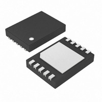
DS2786BG+ Maxim Integrated Products, DS2786BG+ Datasheet - Page 18

DS2786BG+
Manufacturer Part Number
DS2786BG+
Description
IC FUEL GAUGE OCV-BASED 10-TDFN
Manufacturer
Maxim Integrated Products
Specifications of DS2786BG+
Function
Fuel, Gas Gauge/Monitor
Battery Type
Lithium-Ion (Li-Ion), Lithium-Polymer (Li-Pol)
Voltage - Supply
2.5 V ~ 5.5 V
Operating Temperature
-40°C ~ 85°C
Mounting Type
Surface Mount
Package / Case
10-TDFN Exposed Pad
Lead Free Status / RoHS Status
Lead free / RoHS Compliant
Stand-Alone OCV-Based Fuel Gauge
•
•
•
•
•
Location 7Fh provides 1 byte available for storage of
user-defined information. This byte does not affect
operation of the fuel gauge. Factory default is 00h.
The 2-wire bus system supports operation as a slave-
only device in a single or multislave, and single or multi-
master system. The 2-wire interface consists of a serial
data line (SDA) and serial clock line (SCL). SDA and
SCL provide bidirectional communication between the
DS2786B slave device and a master device at speeds
up to 400kHz. The DS2786B’s SDA pin operates bidi-
rectionally; that is, when the DS2786B receives data,
SDA operates as an input, and when the DS2786B
returns data, SDA operates as an open-drain output,
with the host system providing a resistive pullup. The
DS2786B always operates as a slave device, receiving
and transmitting data under the control of a master
device. The master initiates all transactions on the bus
and generates the SCL signal, as well as the START
and STOP bits, which begin and end each transaction.
18
COPY—The Copy bit is set to start a copy command
of the scratchpad to EEPROM. A programming volt-
age must be present on the V
copy to be successful. The Copy bit must be cleared
by software within the t
RCALL—The Recall bit is set to recall the contents
of EEPROM into the scratchpad.
SOCV—Stored OCV calculation. This command can
be used to reset the relative capacity calculation
after updating OCV cell model data in the scratch-
pad. When set to 1, the part is performing an OCV
calculation based on the voltage stored in the Initial
Voltage Register and the OCV lookup table values
present in the scratchpad. Writing the bit to 1 forces
a calculation. Forcing an OCV calculation creates
capacity-estimation error. The bit is cleared when
the hardware completes the calculation.
POCV—Present OCV calculation. When set to 1,
the part is performing an OCV calculation based on
the voltage stored in the Voltage Register and the
OCV lookup table values present in the scratchpad.
Writing the bit to 1 forces a calculation. This func-
tion should be used for test purposes only. Forcing
an OCV calculation creates capacity-estimation
error. The bit is cleared when the hardware com-
pletes the calculation.
POR—Power-on reset. A value of 1 starts a power-
on reset event. The bit is cleared on the next start or
stop on the 2-wire bus, exiting the reset state.
______________________________________________________________________________________
2-Wire Bus System
PROG
time window.
User EEPROM
PROG
pin prior for the
One data bit is transferred during each SCL clock
cycle, with the cycle defined by SCL transitioning low to
high and then high to low. The SDA logic level must
remain stable during the high period of the SCL clock
pulse. Any change in SDA when SCL is high is inter-
preted as a START or STOP control signal.
The bus is defined to be idle, or not busy, when no
master device has control. Both SDA and SCL remain
high when the bus is idle. The STOP condition is the
proper method to return the bus to the idle state.
The master initiates transactions with a START condi-
tion (S) by forcing a high-to-low transition on SDA while
SCL is high. The master terminates a transaction with a
STOP condition (P), a low-to-high transition on SDA
while SCL is high. A Repeated START condition (Sr)
can be used in place of a STOP then START sequence
to terminate one transaction and begin another without
returning the bus to the idle state. In multimaster sys-
tems, a Repeated START allows the master to retain
control of the bus. The START and STOP conditions are
the only bus activities in which the SDA transitions
when SCL is high.
Each byte of a data transfer is acknowledged with an
Acknowledge bit (A) or a No Acknowledge bit (N). Both
the master and the DS2786B slave generate
Acknowledge bits. To generate an acknowledge, the
receiving device must pull SDA low before the rising
edge of the acknowledge-related clock pulse (ninth
pulse) and keep it low until SCL returns low. To gener-
ate a no acknowledge (also called NAK), the receiver
releases SDA before the rising edge of the acknowl-
edge-related clock pulse and leaves SDA high until
SCL returns low. Monitoring the Acknowledge bits
allows for detection of unsuccessful data transfers. An
unsuccessful data transfer can occur if a receiving
device is busy or if a system fault has occurred. In the
event of an unsuccessful data transfer, the bus master
should reattempt communication.
A byte of data consists of 8 bits ordered MSB first. The
LSB of each byte is followed by the Acknowledge bit.
The DS2786B registers composed of multibyte values
are ordered MSB first. The MSB of multibyte registers is
stored on even data memory addresses.
START and STOP Conditions
Acknowledge Bits
Bit Transfer
Data Order
Bus Idle


