ISL94200IRZ Intersil, ISL94200IRZ Datasheet
ISL94200IRZ
Specifications of ISL94200IRZ
Available stocks


Related parts for ISL94200IRZ

ISL94200IRZ Summary of contents
Page 1
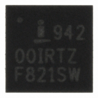
... PART NUMBER PART PACKAGE (Note) MARKING (Pb-free) ISL94200IRZ 942 00IRTZ 24 Ld 4x4 QFN NOTE: These Intersil Pb-free plastic packaged products employ special Pb-free material sets, molding compounds/die attach materials, and 100% matte tin plate plus anneal (e3 termination finish, which is RoHS compliant and compatible with both SnPb and Pb-free soldering operations) ...
Page 2
Pinout Functional Diagram VC7/VCC CELL VCELL6 VOLTAGES VCELL5 LEVEL SHIFTERS VCELL4 VCELL3 VCELL2 VCELL1 BACKUP SUPPLY VSS 2 ISL94200 ISL94200 (24 LD QFN) TOP VIEW VC7/VCC 2 VCELL6 3 VCELL5 4 NC ...
Page 3
Pin Descriptions SYMBOL VC7/VCC Battery cell 7 voltage input/VCC supply. This pin is used to monitor the voltage of this battery cell externally at pin AO. This pin also provides the operating voltage for the IC circuitry. VCELLN Battery cell ...
Page 4
... VCELLN 4 ISL94200 Thermal Information Thermal Resistance (Typical, Notes 1, 2) θ 36. QFN . . . . . . . . . . . . . . . . . . . . . . Continuous Package Power Dissipation . . . . . . . . . . . . . . . . .400mW Storage Temperature . . . . . . . . . . . . . . . . . . . . . . . . . . -55 to +125°C Pb-free Reflow Profile . . . . . . . . . . . . . . . . . . . . . . . . .see link below - 0 0.5V http://www.intersil.com/pbfree/Pb-FreeReflow.asp SS RGO - 22. Operating Conditions - 0. <27V Temperature Range . . . . . . . . . . . . . . . . . . . . . . . . . .-40°C to +85° Supply Voltage Range (Typical 10V Operating Voltage ...
Page 5
Operating Specifications Over the recommended operating conditions unless otherwise specified. Parameters with MIN and/or MAX limits are 100% tested at +25°C, unless otherwise specified. Temperature limits established by characterization and are not production tested. (Continued) PARAMETER SYMBOL OVERCURRENT/SHORT CIRCUIT PROTECTION ...
Page 6
Operating Specifications Over the recommended operating conditions unless otherwise specified. Parameters with MIN and/or MAX limits are 100% tested at +25°C, unless otherwise specified. Temperature limits established by characterization and are not production tested. (Continued) PARAMETER SYMBOL Over Charge Current ...
Page 7
Operating Specifications Over the recommended operating conditions unless otherwise specified. Parameters with MIN and/or MAX limits are 100% tested at +25°C, unless otherwise specified. Temperature limits established by characterization and are not production tested. (Continued) PARAMETER SYMBOL Internal Temperature Monitor ...
Page 8
Operating Specifications Over the recommended operating conditions unless otherwise specified. Parameters with MIN and/or MAX limits are 100% tested at +25°C, unless otherwise specified. Temperature limits established by characterization and are not production tested. (Continued) PARAMETER SYMBOL Start Condition Setup ...
Page 9
Wake-Up Timing (WKPOL = 0) V WKUP2 WKUP PIN t WKUP WKUP BIT Wake up timing (WKPOL = 1) <t V WKUP1 WKUP PIN t WKUP WKUP BIT Change in Voltage Source, FET Control SCL BIT SDA 3 AO DFET ...
Page 10
Automatic Temperature Scan AUTO TEMP CONTROL (INTERNAL ACTIVATION) MONITOR TIME = 5ms TEMP3V PIN EXTERNAL TEMPERATURE OVER-TEMPERATURE TMP3V/13 DELAY TIME = 1ms XOT BIT Discharge Overcurrent/Short Circuit Monitor OCD V DSENSE t SCD ‘0’ DOC BIT ‘0’ ...
Page 11
Charge Overcurrent Monitor V CSENSE V OCC ‘0’ COC BIT TEMP3V OUTPUT 12V CFET OUTPUT µC TURNS ON CFE Serial Interface Timing Diagrams Bus Timing SCL t SU:STA t HD:STA SDA (INPUT TIMING) SDA (OUTPUT TIMING) Symbol Table WAVEFORM INPUTS ...
Page 12
Registers ADDR REGISTER READ/WRITE 00H Config/Op Read only Status 01H Operating Read only Status (Note 10) 02H Not Used Read/Write 03H Analog Out Read/Write 04H FET Control Read/Write 05H Discharge Set Read/Write (Write only if DISSETEN bit set) 06H Charge ...
Page 13
Status Registers BIT FUNCTION 7 RESERVED Reserved for future expansion. 6 RESERVED Reserved for future expansion Indicates the device is an ISL94200. This bit is set in the chip and cannot be changed. Single AFE 4 WKUP This ...
Page 14
Control Registers TABLE 4. ANALOG OUT CONTROL REGISTER (ADDR: 03H) BITS FUNCTION 7 UFLG1 User Flag 1 6 UFLG0 User Flag 0 5:4 RESERVED BIT 3 BIT 2 AO3 AO2 ...
Page 15
TABLE 6. DISCHARGE SET CONFIGURATION REGISTER (ADDR: 05H) SETTING Bit 7 DENOCD Turn off automatic OC discharge control BIT 6 BIT 5 OCDV1 OCDV0 Bit 4 DENSCD Turn off automatic SC discharge ...
Page 16
TABLE 7. CHARGE/TIME SCALE CONFIG REGISTER (ADDR: 06H) SETTING Bit 7 DENOCC Turn off automatic OC charge control BIT 6 BIT 5 OCCV1 OCCV0 Bit 4 SCLONG Short circuit long delay Bit ...
Page 17
BIT FUNCTION 7 FSETEN When set to “1”, allows writes to the Feature Set register. When set to “0”, prevents writes to the Feature Enable discharge set writes Set register (Addr: 07H). Default on initial power up is “0”. ...
Page 18
WKUP Pin Operation There are two ways to design a wake up of the ISL94200 active LOW connection (WKPOL = “0” - default), the device wakes up when a charger is connected to the pack. This pulls the ...
Page 19
VSS OPEN POWER FETs ISL94200 V REF LDFAIL = 1 if VMON >V VMONH ℜ≤ VMON VMON LDMONEN VSS FIGURE 4. LOAD MONITOR CIRCUIT LOAD MONITORING The load monitor function in the ISL94200 (see Figure 4) ...
Page 20
Turning off the FETs in the event of an over-temperature condition prevents continued discharge or charge of the cells when they are over heated. In the event of an automatic over-temperature condition the FETs are held off until the temperature ...
Page 21
External VMON/CFET Protection Mechanisms When there is a single charge/discharge path, a blocking diode is recommended in the VMON to P- path in ISL94200 solution. See D in Figure 7. This diode is to protect against 1 a negative voltage ...
Page 22
In the read mode, the device transmits eight bits of data, releases the SDA line, then monitor the line for an acknowledge acknowledge is detected and no stop condition is generated by the master, the device will continues ...
Page 23
Random Read SLAVE REGISTER R BYTE ADDRESS T SDA BUS Write the CHSETEN bit (Addr 8:bit 6) to “1” to enable changes to the data in ...
Page 24
POWER FAILS AND ONE OR MORE OF THE SUPPLIES, VCC, V AND V CELL3 MAIN OPERATING STATE VOLTAGE REGULATOR IS ON LOGIC AND REGISTERS ARE POWERED BY RGO CFET, DFET OUTPUTS ARE OFF. (REQUIRE AN EXTERNAL COMMAND TO TURN ON) ...
Page 25
Applications Circuits The following application circuits are ideas to consider when developing a battery-pack implementation. There are many more ways that the pack can be designed. ISL94200 0.1µF VC7/VCC VCELL6 VCELL5 VCELL4 VCELL3 VCELL2 4.7µF VCELL1 MINIMIZE LENGTH MAXIMIZE GAUGE ...
Page 26
ISL94200 0.1µF VC7/VCC VCELL6 SCL SDA VCELL5 WKUP RGC VCELL4 RGO TEMP3V VCELL3 TEMPI VCELL2 AO 4.7µF VCELL1 VMON CFET MINIMIZE LENGTH DFET MAXIMIZE GAUGE V SS DSREF OPTIONAL B- FIGURE 15. 7-CELL APPLICATION CIRCUIT SEPARATE CHARGE/DISCHARGE 26 ISL94200 500 ...
Page 27
... Accordingly, the reader is cautioned to verify that data sheets are current before placing orders. Information furnished by Intersil is believed to be accurate and reliable. However, no responsibility is assumed by Intersil or its subsidiaries for its use; nor for any infringements of patents or other rights of third parties which may result from its use ...
Page 28
Package Outline Drawing L24.4x4D 24 LEAD QUAD FLAT NO-LEAD PLASTIC PACKAGE Rev 2, 10/06 4.00 PIN 1 INDEX AREA (4X) 0.15 TOP VIEW ( TYP ) ( TYPICAL RECOMMENDED LAND PATTERN 28 ISL94200 ...