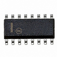
MC33363ADW ON Semiconductor, MC33363ADW Datasheet - Page 7

MC33363ADW
Manufacturer Part Number
MC33363ADW
Description
IC SWIT PROG OVP UVLO HV 16SOIC
Manufacturer
ON Semiconductor
Type
High Voltage Switching Regulatorr
Datasheet
1.MC33363ADWR2G.pdf
(13 pages)
Specifications of MC33363ADW
Output Isolation
Isolated
Frequency Range
59 ~ 315kHz
Voltage - Input
9.5 ~ 40 V
Voltage - Output
700V
Operating Temperature
-25°C ~ 150°C
Package / Case
16-SOIC (0.300", 7.50mm Width) 13 leads
Output Voltage Range
5.5 V to 7.5 V
Input Voltage Range
40 V
Mounting Style
SMD/SMT
Lead Free Status / RoHS Status
Contains lead / RoHS non-compliant
Available stocks
Company
Part Number
Manufacturer
Quantity
Price
Company:
Part Number:
MC33363ADW
Manufacturer:
ON
Quantity:
5 510
Part Number:
MC33363ADW
Manufacturer:
MOTOROLA/摩托罗拉
Quantity:
20 000
Company:
Part Number:
MC33363ADWG
Manufacturer:
ON Semiconductor
Quantity:
20
Part Number:
MC33363ADWR2G
Manufacturer:
ON/安森美
Quantity:
20 000
†For information on tape and reel specifications, including part orientation and tape sizes, please refer to our Tape and Reel Packaging
PIN FUNCTION DESCRIPTION
ORDERING INFORMATION
Specifications Brochure, BRD8011/D.
MC33363ADWG
MC33363ADWR2G
4, 5, 12, 13
14, 15
Pin
10
16
11
1
2
3
6
7
8
9
Voltage Feedback
Regulator Output
Protection Input
Compensation
Power Switch
Startup Input
Overvoltage
Device
Function
V
Drain
GND
Input
CCCC
R
C
--
--
T
T
This pin connects directly to the rectified ac line voltage source. Internally Pin 1 is tied to the drain
of a high voltage startup MOSFET. During startup, the MOSFET supplies internal bias, and
charges an external capacitor that connects from the V
This pin has been omitted for increased spacing between the rectified ac line voltage on Pin 1 and
the V
This is the positive supply voltage input. During startup, power is supplied to this input from Pin 1.
When V
supplied from an auxiliary transformer winding.
These pins are the control circuit grounds. They are part of the IC lead frame and provide a
thermal path from the die to the printed circuit board.
Resistor R
Comparator threshold and affect the Oscillator frequency.
Capacitor C
programs the Oscillator frequency.
This 6.5 V output is available for biasing external circuitry. It requires an external bypass capacitor
of at least 1.0 mF for stability.
This pin is the Error Amplifier output and is made available for loop compensation. It can be used
as an input to directly control the PWM Comparator.
This is the inverting input of the Error Amplifier. It has a 2.6 V threshold and normally connects
through a resistor divider to the converter output, or to a voltage that represents the converter
output.
This input provides runaway output voltage protection due to an external component or
connection failure in the control loop feedback signal path. It has a 2.6 V threshold and normally
connects through a resistor divider to the converter output, or to a voltage that represents the
converter output.
These pins have been omitted for increased spacing between the high voltages present on the
Power Switch Drain, and the ground potential on Pins 12 and 13.
This pin is designed to directly drive the converter transformer and is capable of switching a
maximum of 700 V and 1.0 A.
CC
CC
potential on Pin 3.
T
reaches the UVLO upper threshold, the startup MOSFET turns off and power is
T
connects from this pin to ground. The value selected will program the Current Limit
connects from this pin to ground. The value selected, in conjunction with resistor R
http://onsemi.com
SOIC--16WB
SOIC--16WB
(Pb--Free)
(Pb--Free)
Package
7
Description
CC
pin to ground.
1000 / Tape & Reel
47 Units / Rail
Shipping
†
T
,


