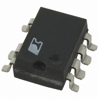
LNK500G-TL Power Integrations, LNK500G-TL Datasheet - Page 2

LNK500G-TL
Manufacturer Part Number
LNK500G-TL
Description
IC SWIT OCP CV/CC HV 8SMD
Manufacturer
Power Integrations
Series
LinkSwitch®r
Datasheet
1.LNK500PN.pdf
(20 pages)
Specifications of LNK500G-TL
Output Isolation
Isolated
Frequency Range
24 ~ 49.5kHz
Voltage - Output
700V
Power (watts)
5.5W
Operating Temperature
-40°C ~ 150°C
Package / Case
8-SMD Gull Wing, 7 Leads
Lead Free Status / RoHS Status
Contains lead / RoHS non-compliant
Figure 2. Block Diagram.
Pin Functional Description
DRAIN (D) Pin:
Power MOSFET drain connection. Provides internal operating
current for start-up. Internal current limit sense point for drain
current.
CONTROL (C) Pin:
Error amplifier and feedback current input pin for duty cycle
and current limit control. Internal shunt regulator connection
to provide internal bias current during normal operation. It is
also used as the connection point for the supply bypass and
auto-restart/compensation capacitor.
SOURCE (S) Pin:
Output MOSFET source connection for high voltage power
return. Primary side control circuit common and reference
point.
2
CONTROL
LNK500
D
2/05
I DCS
R E
Z C
SHUNT REGULATOR/
I
FB
ERROR AMPLIFIER
OSCILLATOR
CLOCK
V C
D MAX
SAW
+
-
5.6 V
COMPARATOR
5.6 V
4.7 V
PW M
+
-
AUTO-RESTART
SHUTDOWN/
+
-
FREQUENCY
OPERATION
LOW
HYSTERETIC
SHUTDOWN
THERMAL
0
1
Figure 3. Pin Configuration.
INTERNAL
SUPPLY
÷ 8
S
R
Q
G Package (SMD-8B)
S
S
S
S
P Package (DIP-8B)
2
3
4
1
LNK500
CURRENT
CURRENT LIMIT
ADJUST
COMPARATOR
BLANKING
LIMIT
LEADING
EDGE
EDGE
8
7
5
+
-
C
D
S
SOURCE
PI-3416-032603
PI-3417-111802
DRAIN


