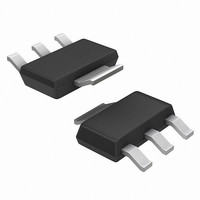
NCP1011ST130T3G ON Semiconductor, NCP1011ST130T3G Datasheet - Page 16

NCP1011ST130T3G
Manufacturer Part Number
NCP1011ST130T3G
Description
IC CTRLR/MOSFET 130KHZ SOT223
Manufacturer
ON Semiconductor
Datasheet
1.NCP1010ST100T3G.pdf
(24 pages)
Specifications of NCP1011ST130T3G
Output Isolation
Isolated
Frequency Range
117 ~ 143kHz
Voltage - Input
8.5 ~ 10 V
Voltage - Output
700V
Power (watts)
19W
Operating Temperature
-40°C ~ 125°C
Package / Case
TO-261-4, TO-261AA, SOT-223-4
Duty Cycle (max)
72 %
Mounting Style
SMD/SMT
Switching Frequency
143 KHz
Operating Supply Voltage
- 0.3 V to + 10 V
Maximum Operating Temperature
+ 150 C
Synchronous Pin
No
Topology
Flyback
Lead Free Status / RoHS Status
Lead free / RoHS Compliant
Other names
NCP1011ST130T3G
NCP1011ST130T3GOSTR
NCP1011ST130T3GOSTR
Available stocks
Company
Part Number
Manufacturer
Quantity
Price
Company:
Part Number:
NCP1011ST130T3G
Manufacturer:
ON Semiconductor
Quantity:
500
Part Number:
NCP1011ST130T3G
Manufacturer:
ON/安森美
Quantity:
20 000
Design Procedure
not differ from that of a standard circuit using a controller
drain at the switch opening cannot be larger than the input
voltage. When selecting components, you thus must adopt
a turn ratio which adheres to the following equation:
operating from a 120 V DC rail, with a delivery of 12 V, we
can select a reflected voltage of 100 Vdc maximum:
120–100 > 0. Therefore, the turn ratio Np:Ns must be
smaller than 100/(12 + 1) = 7.7 or Np:Ns < 7.7. We will see
later on how it affects the calculation.
N · (Vout + Vf) < Vin min
The design of an SMPS around a monolithic device does
As a result, the Flyback voltage which is reflected on the
1. In any case, the lateral MOSFET body- -diode shall
2. A current- -mode architecture is, by definition,
3. Lateral MOSFETs have a poorly dopped
never be forward biased, either during startup
(because of a large leakage inductance) or in
normal operation as shown by Figure 26.
sensitive to subharmonic oscillations.
Subharmonic oscillations only occur when the
SMPS is operating in Continuous Conduction
Mode (CCM) together with a duty- -cycle greater
than 50%. As a result, we recommend to operate
the device in DCM only, whatever duty- -cycle it
implies (max = 65%). However, CCM operation
with duty- -cycles below 40% is possible.
body- -diode which naturally limits their ability to
sustain the avalanche. A traditional RCD clamping
network shall thus be installed to protect the
MOSFET. In some low power applications,
a simple capacitor can also be used since
Vdrain max = Vin + N · (Vout + Vf) + Ip ·
(eq. 15)
, where Lf is the leakage inductance,
--50.0
50.0
350
250
150
(eq. 14)
Figure 26. The Drain- -Source Wave Shall Always be Positive . . .
1.004M
.
For
instance,
1.011M
http://onsemi.com
Ctot
Lf
if
16
1.018M
and a MOSFET. However, one needs to be aware of certain
characteristics specific of monolithic devices:
possible to calculate the maximum power that can be
transferred at low line.
inductance Lp until the current reaches the level imposed by
the feedback loop. The duration of this event is called the ON
time and can be defined by:
to the secondary and the flyback voltage appears across
Lp, resetting the transformer core with a slope of
maximum power, we will not allow a dead- -time after the
core is reset, but rather immediately restart. The switching
time can be expressed by:
N · (Vout + Vf)
> 0 !!
Tsw = toff + ton = Lp · Ip ·
Taking into account all previous remarks, it becomes
When the switch closes, Vin is applied across the primary
At the switch opening, the primary energy is transferred
If one wants to keep DCM only, but still need to pass the
Lp
Ctot is the total capacitance at the drain node
(which is increased by the capacitor wired between
drain and source), N the Np:Ns turn ratio, Vout the
output voltage, Vf the secondary diode forward
drop and finally, Ip the maximum peak current.
Worse case occurs when the SMPS is very close to
regulation, e.g. the Vout target is almost reached
and Ip is still pushed to the maximum.
1.025M
. toff, the OFF time is thus:
toff =
ton =
1.032M
N · (Vout + Vf)
Lp · Ip
Lp · Ip
Vin
Vin
1
+
N · (Vout + Vf)
1
(eq. 16)
(eq. 18)
(eq. 17)


