LNK632DG Power Integrations, LNK632DG Datasheet - Page 3
LNK632DG
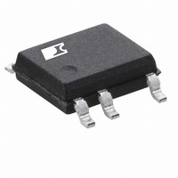
Manufacturer Part Number
LNK632DG
Description
IC SWIT CV/CC HV 8SOIC
Manufacturer
Power Integrations
Series
LinkSwitch®-IIr
Datasheet
1.LNK632DG-TL.pdf
(10 pages)
Specifications of LNK632DG
Output Isolation
Isolated
Frequency Range
98 ~ 112kHz
Voltage - Output
700V
Power (watts)
3.1W
Operating Temperature
-40°C ~ 150°C
Package / Case
8-SOIC (0.154", 3.90mm Width) 7 leads
Lead Free Status / RoHS Status
Lead free / RoHS Compliant
Available stocks
Company
Part Number
Manufacturer
Quantity
Price
Company:

Part Number:
LNK632DG
Manufacturer:
POWER
Quantity:
15 000
Part Number:
LNK632DG
Manufacturer:
POWER
Quantity:
20 000
Part Number:
LNK632DG-TL
Manufacturer:
POWER
Quantity:
20 000


LNK632DG Functional Description
The LNK632DG combines a high voltage power MOSFET
switch with a power supply controller in one device. Similar to
the LinkSwitch-LP and TinySwitch-III it uses a simple ON/OFF
control to regulate the output voltage. In addition, the switching
frequency is modulated to regulate the output current to provide
a constant current characteristic. The LNK632DG controller
consists of an oscillator, feedback (sense and logic) circuit, 6 V
regulator, over-temperature protection, frequency jittering, current
limit circuit, leading-edge blanking, frequency control for constant
current regulation and ON/OFF state machine for CV control.
Constant Current Control (CC) Operation
As the output voltage and therefore the Flyback voltage across
the bias winding ramps up, the feedback pin voltage increases.
The switching frequency is adjusted as the feedback pin voltage
increases to provide a constant output current regulation.
Constant Voltage (CV) Operation
As the feedback pin approaches V
regulation mode, the power supply transitions into CV operation.
The switching frequency at this point is at its maximum value,
corresponding to the peak power point of the CCCV characteristic.
The controller regulates the feedback pin voltage to remain at
V
voltage is sampled 2.5 ms after the turn-off of the high voltage
switch. At light loads the current limit is also reduced to
decrease the transformer flux density.
Output Cable Compensation
This compensation provides a constant output voltage at the
end of the cable over the entire load range in CV mode. As the
converter load increases from no-load to the peak power point
(transition point between CV and CC) the voltage drop introduced
across the output cable is compensated by increasing the
feedback pin reference voltage. The controller determines the
output load and therefore the correct degree of compensation
based on the output of the state machine. Cable drop
compensation for a 26 AWG (0.4 W) cable is selected with C
1 mF and for a 28 AWG (0.75 W) cable with C
Auto-Restart and Open-Loop Protection
In the event of a fault condition such as an output short or an
open loop condition the LNK632DG enters into an appropriate
protection mode as described below.
In the event the feedback pin voltage during the Flyback period
falls below 0.7 V before the feedback pin sampling delay
(~2.5 ms) for a duration in excess of ~300 ms (auto-restart on-
www.powerint.com
FBth
using an ON/OFF state-machine. The feedback pin
FBth
from the constant current
BP
= 10 mF.
BP
=
time (t
power MOSFET is disabled for 1.2 seconds (~20% Auto-Restart
duty cycle). The auto-restart alternately enables and disables
the switching of the power MOSFET until the fault condition is
removed.
In addition to the conditions for auto-restart described above,
if the sensed feedback pin current during the Forward period of
the conduction cycle (switch “on” time) falls below 120 mA, the
converter annunciates this as an open-loop condition (top resistor
in potential divider is open or missing) and reduces the Auto-restart
time from 300 ms to approximately 6 clock cycles (60 ms), whilst
keeping the disable period of 1.2 seconds. This effectively
reduces the Auto-Restart duty cycle to less than 0.05%.
Over-Temperature Protection
The thermal shutdown circuitry senses the die temperature.
The threshold is set at 142 °C typical with a 60 °C hysteresis.
When the die temperature rises above this threshold (142 °C) the
power MOSFET is disabled and remains disabled until the die
temperature falls by 60 °C, at which point the MOSFET is re-
enabled.
Current Limit
The current limit circuit senses the current in the power MOSFET.
When this current exceeds the internal threshold (I
MOSFET is turned off for the remainder of that cycle. The
leading edge blanking circuit inhibits the current limit comparator
for a short time (t
leading edge blanking time has been set so that current spikes
caused by capacitance and rectifier reverse recovery time will not
cause premature termination of the MOSFET conduction.
6 V Regulator
The 6 V regulator charges the bypass capacitor connected to
the BYPASS pin to 6 V by drawing a current from the voltage on
the DRAIN, whenever the MOSFET is off. The BYPASS pin is
the internal supply voltage node. When the MOSFET is on, the
device runs off of the energy stored in the bypass capacitor.
Extremely low power consumption of the internal circuitry
allows the LNK632DG to operate continuously from the current
drawn from the DRAIN pin. A bypass capacitor value of either
1 mF or 10 mF is sufficient for both high frequency decoupling
and energy storage.
Clampless Design Considerations
Ensure that worse-case high line, peak drain voltage is below
the BV
V to allow margin for design variation.
AR-ON
DSS
specification of the internal MOSFET and ideally <650
) the converter enters into Auto-restart, wherein the
LEB
) after the power MOSFET is turned on. This
LNK632DG
LIMIT
), the power
Rev. C 09/09
3
Related parts for LNK632DG
Image
Part Number
Description
Manufacturer
Datasheet
Request
R

Part Number:
Description:
SOP-16
Manufacturer:
Power Integrations
Datasheet:
Part Number:
Description:
DIP8
Manufacturer:
Power Integrations
Datasheet:
Part Number:
Description:
TO-263
Manufacturer:
Power Integrations
Datasheet:
Part Number:
Description:
TO-263
Manufacturer:
Power Integrations
Datasheet:
Part Number:
Description:
Manufacturer:
Power Integrations
Datasheet: