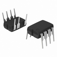
NCP1015AP065G ON Semiconductor, NCP1015AP065G Datasheet - Page 15

NCP1015AP065G
Manufacturer Part Number
NCP1015AP065G
Description
IC OFFLINE SWIT SMPS CM 8DIP
Manufacturer
ON Semiconductor
Datasheet
1.NCP1015AP065G.pdf
(22 pages)
Specifications of NCP1015AP065G
Output Isolation
Isolated
Frequency Range
59 ~ 71kHz
Voltage - Input
8.5 ~ 10 V
Voltage - Output
700V
Power (watts)
19W
Operating Temperature
0°C ~ 150°C
Package / Case
8-DIP (0.300", 7.62mm), 7 Leads
Operating Temperature (max)
150C
Pin Count
7
Mounting
Through Hole
Package Type
PDIP
Case Length
10.16(Max)mm
Case Height
3.44(Max)mm
Output Current
450mA
Output Voltage
700V
No. Of Outputs
1
Supply Voltage Range
6.9V To 9.1V
No. Of Pins
7
Operating Temperature Range
0°C To +125°C
Filter Terminals
Through Hole
Rohs Compliant
Yes
Controller Type, Ic
Current Mode
Lead Free Status / RoHS Status
Lead free / RoHS Compliant
Other names
NCP1015AP065GOS
Available stocks
Company
Part Number
Manufacturer
Quantity
Price
Part Number:
NCP1015AP065G
Manufacturer:
ON/安森美
Quantity:
20 000
V
DRAIN(max)
2. Current−mode architecture is, by definition,
3. Lateral Mosfets have a poorly doped body−diode
As a result, the Flyback voltage which is reflected on
the drain at the switch opening cannot be larger than
the input voltage. When selecting components, you
thus must adopt a turn ratio which adheres to the
following equation:
For instance, if you operate from a 120 V dc rail and
you deliver 12 V, we can select a reflected voltage of
100 VDC maximum: 120 − 100 > 0. Therefore, the
turn ratio Np : Ns must be smaller than 100 / (12 +
1) = 7.7 or Np : Ns < 7.7. We will see later on how
it affects the calculation.
sensitive to subharmonic oscillations.
Subharmonic oscillations only occur when the
SMPS is operating in Continuous Conduction
Mode (CCM) together with a duty−cycle greater
than 50%. As a result, we recommend operating
the device in DCM only, whatever duty−cycle it
implies (max. = 65%).
which naturally limits their ability to sustain the
avalanche. A traditional RCD clamping network
shall thus be installed to protect the MOSFET. In
some low power applications, a simple capacitor
can also be used since:
where L
capacitance at the drain node (which is increased by
the capacitor you will wire between drain and
source), N the Np : Ns turn ratio, V
voltage, V
finally, I
occurs when the SMPS is very close to regulation,
+ V
f
p
N @ (V
in
is the leakage inductance, C
f
the maximum peak current. Worse case
) N @ (V
the secondary diode forward drop and
out
) V
− 50.0
50.0
350
250
150
out
Figure 25. The Drain−Source Wave Shall Always be Positive . . .
f
) V
) t V
1.004M
f
) ) I
IN(min)
p
@
out
C
tot
L
1.011M
tot
the output
f
the total
(eq. 14)
(eq. 15)
http://onsemi.com
15
1.018M
possible to calculate the maximum power that can be
transferred at low line:
inductance L
the feedback loop. The duration of this event is called the ON
time and can be defined by:
to the secondary and the flyback voltage appears across L
reseting the transformer core with a slope of:
the t
maximum power, we will not allow a dead−time after the
core is reset, but rather immediately re−start. The switching
time t
t
which, by extracting I
t
Extracting L
sw
sw
> 0 !!
Taking into account all previous remarks, it becomes
When the switch closes, V
At the switch opening, the primary energy is transferred
If one wants to keep DCM only, but still need to pass the
The Flyback transfer formula dictates that:
+ t
+ L
off
sw
off
time is thus:
e.g. the V
pushed to the maximum.
p
can be expressed by:
1.025M
) t
h @ f
p
p
on
2 @ P
from Equation 20 gives:
until the current reaches the level imposed by
+ L
sw
P
out
h +
out
t
out
@ L
off
p
p
target is almost reached and I
@ I
+
and plugging into Equation 19 leads to:
p
1.032M
t
N @ (V
on
p
@
1
2
N @ (V
@
+
@ L
V
1
in
V
in
L
L
out
L
1
p
in
is applied across the primary
p
p
p
)
V
@ I
out
@ I
@ I
)
) V
in
p
N @ (V
) V
p
p
N @ (V
2
@ f
f
)
@ t
f
sw
)
out
1
off
out
1
) V
) V
f
)
f
)
p
(eq. 16)
(eq. 17)
(eq. 18)
(eq. 19)
(eq. 20)
is still
p
,


