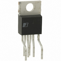
PKS606YN Power Integrations, PKS606YN Datasheet

PKS606YN
Specifications of PKS606YN
Available stocks
Related parts for PKS606YN
PKS606YN Summary of contents
Page 1
PKS603-607 PeakSwitch Enhanced, Energy-Efficient, Off-Line Switcher IC With Super Peak Power Performance Product Highlights ® EcoSmart – Extremely Energy-Efficient • Standby output power ≥0.6 W for 1 W input (high line) • Sleep mode power ≥2 input (high line) • No-load consumption <200 mW at 265 VAC input • Surpasses California Energy Commission (CEC), ENERGY STAR, and EU requirements PeakSwitch Features Reduce System Cost • Delivers peak power three times maximum continuous output power • 277 kHz operation during peak power significantly reduces transformer size • ...
Page 2
PKS603-607 BYPASS (BP) LINE UNDER-VOLTAGE 240 µA 25 µA LATCH OFF/ RESTART COUNTER ON TIME EXT 6.3 V ENABLE JITTER 1 OSCILLATOR ENABLE/ 1.0 V UNDER- VOLTAGE (EN/UV) Figure 2. Functional Block Diagram. Pin Functional Description ...
Page 3
PeakSwitch Functional Description PeakSwitch integrates a 700 V power MOSFET switch with a power supply controller on the same die. Unlike conventional pulse width modulation (PWM) controllers, PeakSwitch uses a simple ON/OFF control to regulate the output voltage. The controller consists of an oscillator, enable circuit (sense and logic), current-limit state machine, 5.8 V regulator, BYPASS pin under-voltage circuit, over- temperature protection, current limit circuit, and leading edge blanking. PeakSwitch incorporates ...
Page 4
...
Page 5
V 300 DRAIN 200 100 DC-OUTPUT Time (s) Figure 6. PeakSwitch Auto-Restart Operation. the line under-voltage sense circuit prevents a restart attempt until the AC input voltage is removed (I <25 µA). Then the internal auto-restart latch is reset and EN the power MOSFET switching will resume once the AC input ...
Page 6
...
Page 7
V DC-INPUT BYPASS 0 Modifying current schematic 300 200 100 V DRAIN Time (ms) Figure 12. PeakSwitch Power Up Without Optional External UV Resistor Connected to EN/UV Pin. 200 V 100 0 400 300 ...
Page 8
...
Page 9
This protects the load and supply from a continuous fault condition. Removing the AC input resets this condition. The output voltage is determined by the Zener diode VR2, the voltage drop across R12 and the forward drop of D9 and the LED of optocoupler U2. Resistor R13 provides bias current through D9 and VR2, to ensure that VR2 is operating close to its knee voltage, while R12 sets the overall gain of the feedback loop. Capacitor C15 boosts high frequency loop gain to help distribute the enabled switching cycles and reduce pulse grouping. When the output voltage exceeds the feedback threshold voltage, current will flow in the optocoupler LED, causing current flow in the transistor of the optocoupler. W hen this exceeds the ENABLE pin threshold current the next switching cycle is inhibited, as the output voltage falls (below the feedback threshold) a conduction cycle is allowed to occur and by adjusting the number of enabled cycles output regulation is maintained. As the load reduces the number of enabled cycles decreases, lowering the effective switching frequency and scaling switching losses with load. This provides almost constant efficiency down to very light loads, ideal for meeting energy efficiency requirements. PeakSwitch device U1 is supplied from an auxillary winding on the transformer which is rectified and filtered by D7 and C6. Resistor R7 provides approximately supply current into the BYPASS pin capacitor C8. During startup or fault conditions when the bias voltage is low, the BYPASS pin is supplied from ...
Page 10
...
Page 11
Input Filter Capacitor TOP VIEW + Input Filter Capacitor HV - TOP VIEW Heat Sink Figure 17. Recommended Layout for PeakSwitch in (a) P and (b) Y/F Packages. Safety Spacing PRI T r BIAS ...
Page 12
...
Page 13
DRAIN Voltage .................................. . .............-0 700 V DRAIN Peak Current: ....................... . ..... 2 × I EN/UV Voltage ....................................................-0 EN/UV Current .................................................... ....... 100 mA BYPASS Voltage .................................................. - 0 Storage Temperature ......................................-65 °C to 150 °C Operating Junction Temperature .................-40 °C to 150 °C (2) Lead Temperature ................ . ...................................... 260 °C (3) Thermal Impedance: Y/F Package ........................................80 °C/W ( ..........................................2 °C/W ( Package: ...
Page 14
...
Page 15
Parameter Symbol CIRCUIT PROTECTION (cont.) Initial Current Limit I INIT Leading Edge t Blanking Time LEB Current Limit t Delay ILD Thermal Shutdown Temperature Thermal Shutdown Hysteresis OUTPUT ON-State R Resistance DS(ON) I DSS1 OFF-State Drain Leakage Current I DSS2 ...
Page 16
...
Page 17
EN/ NOTE: This test circuit is not applicable for current limit or output characteristic measurements. Figure 18. PeakSwitch General Test Circuit. Figure 19. Duty Cycle Measurement. 470 470 ...
Page 18
...
Page 19
Typical Performance Characteristics (cont.) 1.2 1 0.8 0.6 0.4 0 Junction Temperature (°C) Figure 28. Under-Voltage Threshold vs. Temperature. 100 150 Figure 29. Maximum Allowable Drain Current vs. PKS603-607 2.5 2 1 ...
Page 20
...
Page 21
D S .004 (.10) -E- .240 (6.10) .260 (6.60) Pin 1 .367 (9.32) -D- .387 (9.83) .125 (3.18) .145 (3.68) -T- SEATING PLANE .100 (2.54) BSC .048 (1.22) .053 (1.35) .014 (.36) ⊕ .010 (.25) ...
Page 22
...
Page 23
PKS603-607 23 Rev. I 02/07 ...
Page 24
... A critical component is any component of a life support device or system whose failure to perform can be reasonably expected to cause the failure of the life support device or system affect its safety or effectiveness. The PI logo, TOPSwitch, TinySwitch, LinkSwitch, DPA-Switch, PeakSwitch, Clampless, EcoSmart, E-Shield, Filterfuse, StackFET, PI Expert and PI FACTS are trademarks of Power Integrations, Inc. Other trademarks are property of their respective companies. ©Copyright 2007, Power Integrations, Inc. Power Integrations Worldwide Sales Support Locations WORLD HEADQUARTERS GERMANY 5245 Hellyer Avenue Rueckertstrasse 3 San Jose, CA 95138, USA ...


