TOP267VG Power Integrations, TOP267VG Datasheet - Page 10
TOP267VG
Manufacturer Part Number
TOP267VG
Description
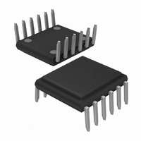
IC OFFLINE SW PWM OCP OVP 12EDIP
Manufacturer
Power Integrations
Series
TOPSwitch®-JXr
Type
Off Line Switcherr
Datasheet
1.TOP264EG.pdf
(40 pages)
Specifications of TOP267VG
Output Isolation
Isolated
Frequency Range
66 ~ 132kHz
Voltage - Output
725V
Power (watts)
32W
Operating Temperature
-40°C ~ 150°C
Package / Case
12-SDIP (0.412", 10.46mm) Exposed Pad
Output Voltage
12 V
Switching Frequency
132 KHz, 66 KHz
Supply Current
3.1 mA, 3.4 mA
Operating Temperature Range
- 40 C to + 150 C
Mounting Style
Through Hole
Maximum Operating Temperature
+ 150 C
Minimum Operating Temperature
- 40 C
Output Power
19 W, 32 W
Lead Free Status / RoHS Status
Lead free / RoHS Compliant
Other names
596-1275-5
Available stocks
Company
Part Number
Manufacturer
Quantity
Price

Part Number:
TOP267VG
Manufacturer:
POWER
Quantity:
20 000


Shutdown/Auto-Restart (for OCP, SCP, OPP)
To minimize TOP264-271 power dissipation under fault
conditions such as over current (OC), short-circuit (SC) or over
power (OP), the shutdown/auto-restart circuit turns the power
supply on and off at an auto-restart duty cycle of typically 2% if
an out of regulation condition persists. Loss of regulation
interrupts the external current into the CONTROL pin. V
regulation changes from shunt mode to the hysteretic auto-
restart mode as described in CONTROL pin operation section.
When the fault condition is removed, the power supply output
becomes regulated, V
normal operation of the power supply resumes.
Hysteretic Over-Temperature Protection (OTP)
Temperature protection is provided by a precision analog circuit
that turns the output MOSFET off when the junction temperature
exceeds the thermal shutdown temperature (142 °C typical).
When the junction temperature cools to below the lower
hysteretic temperature point, normal operation resumes, thus
providing automatic recovery. A large hysteresis of 75 °C
(typical) is provided to prevent overheating of the PC board due
to a continuous fault condition. V
mode, and a 4.8 V to 5.8 V (typical) triangular waveform is
present on the CONTROL pin while in thermal shutdown.
Rev. C 11/10
10
TOP264-271
C
regulation returns to shunt mode, and
C
is regulated in hysteretic
C
Bandgap Reference
All critical TOP264-271 internal voltages are derived from a
temperature-compensated bandgap reference. This voltage
reference is used to generate all other internal current references,
which are trimmed to accurately set the switching frequency,
MOSFET gate drive current, current limit, and the line OV/UV/
OVP thresholds. TOP264-271 has improved circuitry to
maintain all of the above critical parameters within very tight
absolute and temperature tolerances.
High-Voltage Bias Current Source
This high-voltage current source biases TOP264-271 from the
DRAIN pin and charges the CONTROL pin external capacitance
during start-up or hysteretic operation. Hysteretic operation
occurs during auto-restart, remote OFF and over-temperature
shutdown. In this mode of operation, the current source is
switched on and off, with an effective duty cycle of approxi-
mately 35%. This duty cycle is determined by the ratio of
CONTROL pin charge (I
This current source is turned off during normal operation when
the output MOSFET is switching. The effect of the current
source switching will be seen on the DRAIN voltage waveform
as small disturbances and is normal.
C
) and discharge currents (I
www.powerint.com
CD1
and I
CD2
).
Related parts for TOP267VG
Image
Part Number
Description
Manufacturer
Datasheet
Request
R

Part Number:
Description:
SOP-16
Manufacturer:
Power Integrations
Datasheet:
Part Number:
Description:
DIP8
Manufacturer:
Power Integrations
Datasheet:
Part Number:
Description:
TO-263
Manufacturer:
Power Integrations
Datasheet:
Part Number:
Description:
TO-263
Manufacturer:
Power Integrations
Datasheet:
Part Number:
Description:
Manufacturer:
Power Integrations
Datasheet: