DS1216B Maxim Integrated Products, DS1216B Datasheet - Page 4
DS1216B
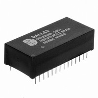
Manufacturer Part Number
DS1216B
Description
IC SMARTWATCH RAM 16K/64K 28SOIC
Manufacturer
Maxim Integrated Products
Datasheet
1.DS1216C.pdf
(14 pages)
Specifications of DS1216B
Controller Type
Smartwatch RAM
Voltage - Supply
4.5 V ~ 5.5 V
Operating Temperature
0°C ~ 70°C
Package / Case
28-DIP (0.600", 15.24mm) Socket
Lead Free Status / RoHS Status
Contains lead / RoHS non-compliant
Available stocks
Company
Part Number
Manufacturer
Quantity
Price


comparison register and awaits the next write cycle. If a match is not found, the pointe
and all subsequent write cycles are ignored. If a read cycle occurs at any time during p
the present sequence is aborted and the comparison register pointer is reset. Pattern rec
for 64 write cycles as described above until all the bits in the comparison register have been m
bit pattern is shown in Figure 1). With a correct match for 64 bits, the SmartWatch i
transfer to or from the timekeeping registers can proceed. The next 64 cycles will cause the Sm
to either receive or transmit data on DQ0, depending on the level of the OE pin or the
other locations outside the memory block can be interleaved with CE cycles witho
pattern recognition sequence or data transfer sequ
PATTERN MATCH—ROM
Communication with the SmartWatch is established by pattern recognition of
that must be matched by executing 64 consecutive write cycles, placing address bi
proper data on address bit A0. The 64 write cycles are used only to gain access to the
to executing the first of 64 write cycles, a read cycle should be executed by holding
cycle will reset the comparison register poi
starts with the
the 64-bit comparison register. If a match is found, the pointer increments to the n
comparison register and awaits the next write cycle. If a match is not found, the pointe
and all subsequent write cycles are ignored. If a read cycle occurs at any time during p
the present sequence is aborted and the comparison register pointer is reset. Pattern rec
for a total of 64 write cycles as described above, until all the bits in the comparison
matched (this bit pattern is shown in Figure 1). With a correct match for 64 bits,
enabled and data transfer to or from the timekeeping registers can proceed. The next 6
the SmartWatch to either receive data on data in (A0) or transmit data on data out (D
the leve
After power-up, the controller could be in the 64-bit clock register read/write sequence (from
incomplete access prior to power-down). Therefore, it is recommended that a 64-bit
upon power-up to prevent accidental writes to the clock, and to prevent reading clock d
the RAM would otherwise be expected.
l of /WRITE READ (A2).
first bit of the sequence. When the first write cycle is executed, it is compared to bit 0 of
nter within the SmartWatch, ensuring the pattern recognition
ence to the SmartWatch.
4 of 14
DS1216 SmartWatch RAM/SmartWatch ROM
a serial bit stream of 64 bits
ext location of the
the SmartWatch is
t A2 low with the
s enabled and data
4 cycles will cause
Q0), depending on
r does not advance
ut interrupting the
SmartWatch. Prior
r does not advance
A2 high. The read
read be performed
ognition continues
ognition continues
register have been
ata when access to
WE pin. Cycles to
attern recognition,
attern recognition,
atched (this
artWatch
an
Related parts for DS1216B
Image
Part Number
Description
Manufacturer
Datasheet
Request
R

Part Number:
Description:
MAX7528KCWPMaxim Integrated Products [CMOS Dual 8-Bit Buffered Multiplying DACs]
Manufacturer:
Maxim Integrated Products
Datasheet:
Part Number:
Description:
Single +5V, fully integrated, 1.25Gbps laser diode driver.
Manufacturer:
Maxim Integrated Products
Datasheet:
Part Number:
Description:
Single +5V, fully integrated, 155Mbps laser diode driver.
Manufacturer:
Maxim Integrated Products
Datasheet:
Part Number:
Description:
VRD11/VRD10, K8 Rev F 2/3/4-Phase PWM Controllers with Integrated Dual MOSFET Drivers
Manufacturer:
Maxim Integrated Products
Datasheet:
Part Number:
Description:
Highly Integrated Level 2 SMBus Battery Chargers
Manufacturer:
Maxim Integrated Products
Datasheet:
Part Number:
Description:
Current Monitor and Accumulator with Integrated Sense Resistor; ; Temperature Range: -40°C to +85°C
Manufacturer:
Maxim Integrated Products
Part Number:
Description:
TSSOP 14/A�/RS-485 Transceivers with Integrated 100O/120O Termination Resis
Manufacturer:
Maxim Integrated Products
Part Number:
Description:
TSSOP 14/A�/RS-485 Transceivers with Integrated 100O/120O Termination Resis
Manufacturer:
Maxim Integrated Products
Part Number:
Description:
QFN 16/A�/AC-DC and DC-DC Peak-Current-Mode Converters with Integrated Step
Manufacturer:
Maxim Integrated Products
Part Number:
Description:
TDFN/A/65V, 1A, 600KHZ, SYNCHRONOUS STEP-DOWN REGULATOR WITH INTEGRATED SWI
Manufacturer:
Maxim Integrated Products
Part Number:
Description:
Integrated Temperature Controller f
Manufacturer:
Maxim Integrated Products
Part Number:
Description:
SOT23-6/I�/45MHz to 650MHz, Integrated IF VCOs with Differential Output
Manufacturer:
Maxim Integrated Products
Part Number:
Description:
SOT23-6/I�/45MHz to 650MHz, Integrated IF VCOs with Differential Output
Manufacturer:
Maxim Integrated Products
Part Number:
Description:
EVALUATION KIT/2.4GHZ TO 2.5GHZ 802.11G/B RF TRANSCEIVER WITH INTEGRATED PA
Manufacturer:
Maxim Integrated Products
Part Number:
Description:
QFN/E/DUAL PCIE/SATA HIGH SPEED SWITCH WITH INTEGRATED BIAS RESISTOR
Manufacturer:
Maxim Integrated Products
Datasheet: