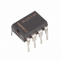
DS1312 Maxim Integrated Products, DS1312 Datasheet

DS1312
Specifications of DS1312
Available stocks
Related parts for DS1312
DS1312 Summary of contents
Page 1
... Industrial temperature range of -40°C to +85°C DESCRIPTION The DS1312 Nonvolatile Controller with Battery Monitor is a CMOS circuit which solves the application problem of converting CMOS RAM into nonvolatile memory. Incoming power is monitored for an out- of-tolerance condition. When such a condition is detected, chip enable is inhibited to accomplish write protection and the battery is switched on to supply the RAM with uninterrupted power ...
Page 2
... As a result, the Battery Warning pin is activated to signal the need for battery replacement. MEMORY BACKUP The DS1312 performs all the circuit functions required to provide battery-backup for an SRAM. First, the device provides a switch to direct power from the battery or the system power supply (V V ...
Page 3
... NOTE: The DS1312 cannot constantly monitor an attached battery because such monitoring would drastically reduce the life of the battery result, the DS1312 only tests the battery for one second out of every 24 hours and does not monitor the battery in any way between tests good battery (one that ...
Page 4
FUNCTIONAL BLOCK DIAGRAM Figure ...
Page 5
ABSOLUTE MAXIMUM RATINGS* Voltage on Any Pin Relative to Ground Operating Temperature Storage Temperature Soldering Temperature * This is a stress rating only and functional operation of the device at these or any other conditions above those indicated in the ...
Page 6
CAPACITANCE PARAMETER Input Capacitance ( , TOL) CEI Output Capacitance ( , , ) CEO BW RST AC ELECTRICAL CHARACTERISTICS PARAMETER to Propagation Delay CEI CEO Pulse Width CE V Valid to End of CC Write Protection V Valid to ...
Page 7
TIMING DIAGRAM: POWER-UP NOTE < will begin to slew with V BAT SW CCO when CCI CCI BAT ...
Page 8
TIMING DIAGRAM: POWER-DOWN NOTE < will slew down with V BAT SW CCO until CCI CCI BAT ...
Page 9
TIMING DIAGRAM: BATTERY WARNING DETECTION NOTE measured from the expiration of the internal timer to the activation of the battery warning output TIMING DIAGRAM: BATTERY REPLACEMENT ...
Page 10
... DS1312 can supply to attached memories at V CCO1 V -0.3V. CCI 5. All inputs within 0.3V of ground the maximum average load current which the DS1312 can supply to the memories in the CCO2 battery backup mode. 7. Measured with a load as shown in Figure 2. 8. Chip Enable Output CEO 9. ...
Page 11
... The following represent the key differences between 06/12/97 and 08/29/97 version of the DS1312 data sheet. Please review this summary carefully. 1. Changed AC test conditions The following represent the key differences between 08/29/97 and 12/16/97 version of the DS1312 data sheet. Please review this summary carefully. 1. Specified Input Capacitance as being only for ...


