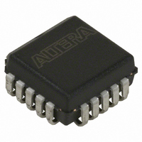
EPC1441LC20N Altera, EPC1441LC20N Datasheet - Page 17

EPC1441LC20N
Manufacturer Part Number
EPC1441LC20N
Description
IC CONFIG DEVICE 440KBIT 20-PLCC
Manufacturer
Altera
Series
EPCr
Datasheet
1.EPC1PC8.pdf
(26 pages)
Specifications of EPC1441LC20N
Programmable Type
OTP
Memory Size
440kb
Voltage - Supply
3 V ~ 3.6 V, 4.75 V ~ 5.25 V
Operating Temperature
0°C ~ 70°C
Package / Case
20-PLCC
Function
Configuration Device
Frequency (max)
16.7MHz
Operating Supply Voltage (typ)
3.3/5V
Operating Supply Voltage (max)
5.25V
Operating Supply Voltage (min)
3V
Operating Temperature Classification
Commercial
Operating Temperature (min)
0C
Operating Temperature (max)
70C
Mounting
Surface Mount
Pin Count
20
Package Type
PLCC
Memory Type
Flash
Supply Voltage Range
3V To 5.25V
Memory Case Style
LCC
No. Of Pins
20
Operating Temperature Range
0°C To +70°C
Filter Terminals
SMD
Rohs Compliant
Yes
Digital Ic Case Style
LCC
For Use With
PLMJ1213 - PROGRAMMER ADAPTER 20 PIN J-LEAD
Lead Free Status / RoHS Status
Lead free / RoHS Compliant
Other names
544-1371-5
EPC1441LC20N
EPC1441LC20N
Available stocks
Company
Part Number
Manufacturer
Quantity
Price
Company:
Part Number:
EPC1441LC20N
Manufacturer:
AMD
Quantity:
1 200
Part Number:
EPC1441LC20N
Manufacturer:
ALTERA/阿尔特拉
Quantity:
20 000
Chapter 4: Configuration Devices for SRAM-Based LUT Devices Data Sheet
Timing Information
Table 4–9. Timing Parameters when Using EPC1 and EPC1441 Devices at 3.3 V
Table 4–10. Timing Parameters when Using EPC1, EPC2 and EPC1441 Devices at 5.0 V (Part 1 of 2)
© December 2009
t
t
t
t
t
t
t
f
t
t
t
t
t
t
t
t
t
Note to
(1) During initial power-up, a POR delay occurs to permit voltage levels to stabilize. Subsequent reconfigurations do not incur this delay.
t
t
t
t
t
t
t
f
t
t
POR
OEZX
CE
DSU
DH
CO
CDOE
CLK
MCH
MCL
SCH
SCL
CASC
CCA
OEW
OEC
NRCAS
POR
OEZX
CE
DSU
DH
CO
CDOE
CLK
MCH
MCL
Symbol
Symbol
Table
4–9:
POR delay
OE high to DATA output enabled
OE high to first rising edge on DCLK
Data setup time before rising edge on DCLK
Data hold time after rising edge on DCLK
DCLK to DATA out
DCLK to DATA enable/disable
DCLK frequency
DCLK high time for the first device in the configuration
chain
DCLK low time for the first device in the configuration
chain
DCLK high time for subsequent devices
DCLK low time for subsequent devices
DCLK rising edge to nCASC
nCS to nCASC cascade delay
OE low pulse width (reset) to guarantee counter reset
OE low (reset) to DCLK disable delay
OE low (reset) to nCASC delay
Altera Corporation
Table 4–9
3.3 V.
Table 4–10
devices at 5.0 V.
(1)
(1)
defines the timing parameters when using EPC1 and EPC1441 devices at
Parameter
defines the timing parameters when using EPC1, EPC2, and EPC1441
Parameter
Min
100
—
—
—
30
—
—
50
50
50
50
—
—
—
—
0
2
Min
6.7
—
—
—
30
—
—
30
30
0
Configuration Handbook (Complete Two-Volume Set)
125
125
Typ
—
—
—
—
—
—
—
—
—
—
—
—
—
—
4
Typ
—
—
—
—
—
—
—
10
50
50
Max
200
300
250
250
80
—
—
30
30
10
—
—
25
15
—
30
30
Max
16.7
200
200
50
—
—
20
20
75
75
Units
Units
MHz
MHz
ms
ns
ns
ns
ns
ns
ns
ns
ns
ns
ns
ns
ns
ns
ns
ns
ms
ns
ns
ns
ns
ns
ns
ns
ns
4–17


