EPC16UC88N Altera, EPC16UC88N Datasheet - Page 21
EPC16UC88N
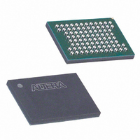
Manufacturer Part Number
EPC16UC88N
Description
IC CONFIG DEVICE 16MBIT 88-UBGA
Manufacturer
Altera
Series
EPCr
Specifications of EPC16UC88N
Programmable Type
In System Programmable
Memory Size
16Mb
Voltage - Supply
3 V ~ 3.6 V
Operating Temperature
0°C ~ 70°C
Package / Case
88-UBGA
Function
Configuration Device
Operating Supply Voltage (typ)
3.3V
Operating Supply Voltage (max)
3.6V
Operating Supply Voltage (min)
3V
Operating Temperature Classification
Commercial
Operating Temperature (min)
0C
Operating Temperature (max)
70C
Mounting
Surface Mount
Pin Count
88
Package Type
uBGA
Memory Type
Flash
Clock Frequency
66.7MHz
Supply Voltage Range
3V To 3.6V
Memory Case Style
BGA
No. Of Pins
88
Operating Temperature Range
0°C To +70°C
Access Time
90ns
Rohs Compliant
Yes
Lead Free Status / RoHS Status
Lead free / RoHS Compliant
Other names
544-1374
EPC16UC88N
EPC16UC88N
Available stocks
Company
Part Number
Manufacturer
Quantity
Price
Company:

Part Number:
EPC16UC88N
Manufacturer:
ALTERA
Quantity:
35
Company:
Part Number:
EPC16UC88N
Manufacturer:
ALTERA31EOL
Quantity:
184
Part Number:
EPC16UC88N
Manufacturer:
ALTERA/阿尔特拉
Quantity:
20 000


Chapter 1: Enhanced Configuration Devices (EPC4, EPC8, and EPC16) Data Sheet
Pin Description
Pin Description
Table 1–8. Configuration Interface Pins (Part 1 of 2)
© December 2009 Altera Corporation
DATA[7..0]
DCLK
Pin Name
f
1
An initiate configuration (nINIT_CONF) JTAG instruction can be added to your
programming file in the Quartus II software by enabling the Initiate configuration
after programming option in the Programmer options window (Options menu).
Programming via External Flash Interface
This method allows parallel programming of the flash memory (using the 16-bit data
bus). An external processor or FPGA acts as the flash controller and has access to
programming data (via a communication link such as UART, Ethernet, and PCI). In
addition to the program, erase, and verify operations, the external flash interface
supports block/sector protection instructions.
For information about protection commands, areas, and lock bits, refer to the
appropriate flash data sheets.
■
■
■
External flash interface programming is only allowed when the configuration
controller has relinquished flash access (by tri-stating its internal interface). If the
controller has not relinquished flash access (during configuration or JTAG-based ISP),
you must hold the controller in reset before initiating external programming. The
controller can be reset by holding the FPGA nCONFIG line at a logic low level. This
keeps the controller in reset by holding the nSTATUS-OE line low, allowing external
flash access.
If initial programming of the enhanced configuration device is done in-system via the
external flash interface, the controller must be kept in reset by driving the FPGA
nCONFIG line low to prevent contention on the flash interface.
Table 1–8
tables include configuration interface pins, external flash interface pins, JTAG
interface pins, and other pins.
Pin Type
Output
Output
For Micron flash-based EPC4, refer to the Micron Flash Memory MT28F400B3 Data
Sheet at www.micron.com.
For Sharp flash-based EPC16, refer to the Sharp LHF16J06 Data Sheet Flash Memory
Used in EPC16 Devices at www.sharpsma.com.
For the Intel Advanced Boot Block Flash Memory (B3) 28F008/800B3, 28F016/160B3,
28F320B3, 28F640B3 Datasheet, visit www.intel.com.
through
Configuration data output bus. DATA changes on each falling edge of DCLK.
DATA is latched into the FPGA on the rising edge of DCLK.
The DCLK output pin from the enhanced configuration device serves as the FPGA
configuration clock. DATA is latched by the FPGA on the rising edge of DCLK.
Table 1–10
describe the enhanced configuration device pins. These
Description
Configuration Handbook (Complete Two-Volume Set)
1–21
Related parts for EPC16UC88N
Image
Part Number
Description
Manufacturer
Datasheet
Request
R

Part Number:
Description:
Configuration EPROMs For Flex Devices
Manufacturer:
Altera Corporation
Datasheet:

Part Number:
Description:
CYCLONE II STARTER KIT EP2C20N
Manufacturer:
Altera
Datasheet:

Part Number:
Description:
CPLD, EP610 Family, ECMOS Process, 300 Gates, 16 Macro Cells, 16 Reg., 16 User I/Os, 5V Supply, 35 Speed Grade, 24DIP
Manufacturer:
Altera Corporation
Datasheet:
Part Number:
Description:
CPLD, EP610 Family, ECMOS Process, 300 Gates, 16 Macro Cells, 16 Reg., 16 User I/Os, 5V Supply, 15 Speed Grade, 24DIP
Manufacturer:
Altera Corporation
Datasheet:
Part Number:
Description:
Manufacturer:
Altera Corporation
Datasheet:
Part Number:
Description:
CPLD, EP610 Family, ECMOS Process, 300 Gates, 16 Macro Cells, 16 Reg., 16 User I/Os, 5V Supply, 30 Speed Grade, 24DIP
Manufacturer:
Altera Corporation
Datasheet:
Part Number:
Description:
High-performance, low-power erasable programmable logic devices with 8 macrocells, 10ns
Manufacturer:
Altera Corporation
Datasheet:
Part Number:
Description:
High-performance, low-power erasable programmable logic devices with 8 macrocells, 7ns
Manufacturer:
Altera Corporation
Datasheet:
Part Number:
Description:
Classic EPLD
Manufacturer:
Altera Corporation
Datasheet:
Part Number:
Description:
High-performance, low-power erasable programmable logic devices with 8 macrocells, 10ns
Manufacturer:
Altera Corporation
Datasheet:
Part Number:
Description:
Manufacturer:
Altera Corporation
Datasheet:
Part Number:
Description:
Manufacturer:
Altera Corporation
Datasheet:
Part Number:
Description:
Manufacturer:
Altera Corporation
Datasheet: