EPC16UC88N Altera, EPC16UC88N Datasheet - Page 24
EPC16UC88N
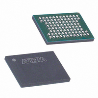
Manufacturer Part Number
EPC16UC88N
Description
IC CONFIG DEVICE 16MBIT 88-UBGA
Manufacturer
Altera
Series
EPCr
Specifications of EPC16UC88N
Programmable Type
In System Programmable
Memory Size
16Mb
Voltage - Supply
3 V ~ 3.6 V
Operating Temperature
0°C ~ 70°C
Package / Case
88-UBGA
Function
Configuration Device
Operating Supply Voltage (typ)
3.3V
Operating Supply Voltage (max)
3.6V
Operating Supply Voltage (min)
3V
Operating Temperature Classification
Commercial
Operating Temperature (min)
0C
Operating Temperature (max)
70C
Mounting
Surface Mount
Pin Count
88
Package Type
uBGA
Memory Type
Flash
Clock Frequency
66.7MHz
Supply Voltage Range
3V To 3.6V
Memory Case Style
BGA
No. Of Pins
88
Operating Temperature Range
0°C To +70°C
Access Time
90ns
Rohs Compliant
Yes
Lead Free Status / RoHS Status
Lead free / RoHS Compliant
Other names
544-1374
EPC16UC88N
EPC16UC88N
Available stocks
Company
Part Number
Manufacturer
Quantity
Price
Company:

Part Number:
EPC16UC88N
Manufacturer:
ALTERA
Quantity:
35
Company:
Part Number:
EPC16UC88N
Manufacturer:
ALTERA31EOL
Quantity:
184
Part Number:
EPC16UC88N
Manufacturer:
ALTERA/阿尔特拉
Quantity:
20 000


1–24
Table 1–9. External Flash Interface Pins (Part 2 of 2)
Table 1–10. JTAG Interface Pins and Other Required Controller Pins (Part 1 of 2)
Volume 2: Configuration Handbook
WP#
V
RY/BY#
BYTE#
Notes to
(1) These pins can be driven to 12 V during production testing of the flash memory. Since the controller cannot tolerate the 12-V level, connections
(2) For more information, refer to the Process Change Notification
TDI
TDO
TCK
TMS
PGM[2..0]
CCW
Pin Name
Pin Name
from the controller to these pins are not made internal to the package. Instead they are available as two separate pins. You must connect the
two pins at the board level (for example, on the printed circuit board (PCB), connect the C-WE# pin from controller to F-WE# pin from the flash
memory).
Enhanced Configuration Devices
Table
1–9:
Open-Drain Output
Pin Type
Pin Type
Supply
Output
Input
Input
Input
Input
Input
Input
and
Using the Intel Flash Memory-Based EPC4, EPC8 and EPC16
Usually tied to V
because it could cause contention.
Connection to V
to allow programming of the flash-bottom boot block, which is required when
programming the device using the Quartus II software.
This pin should be connected to V
used.
Block erase, full-chip erase, word write, or lock-bit configuration power supply.
Connect this pin to the 3.3-V V
flash interface.
Flash asserts this pin when a write or erase operation is complete. This pin is not
connected to the controller. RY/BY# is only available in Sharp flash-based EPC8
and EPC16.
Leave this pin floating when the external flash interface is not used.
Flash byte-enable pin and is only available for enhanced configuration devices in
the 100-pin PQFP package.
This pin must be connected to V
external flash interface (the controller uses the flash in 16-bit mode). For Intel
flash-based EPC device, this pin is connected to the V
internally. Therefore, BYTE# must be connected directly to V
pull-up resistor.
JTAG data input pin.
Connect this pin to V
JTAG data output pin.
Do not connect this pin if the JTAG circuitry is not used (leave floating).
JTAG clock pin.
Connect this pin to GND if the JTAG circuitry is not used.
JTAG mode select pin.
Connect this pin to V
These three input pins select one of the eight pages of configuration data to
configure the FPGAs in the system.
Connect these pins on the board to select the page specified in the Quartus II
software when generating the enhanced configuration device POF. PGM[2] is the
MSB. The default selection is page 0; PGM[2..0]=000. These pins must not be
left floating.
Chapter 1: Enhanced Configuration Devices (EPC4, EPC8, and EPC16) Data Sheet
(2)
PCN0506: Addition of Intel Flash Memory As Source For EPC4, EPC8 and EPC16
CC
CC
is recommended for faster block erase/programming times and
or ground on the board. The controller does not drive this pin
CC
CC
if the JTAG circuitry is not used.
if the JTAG circuitry is not used.
CC
CC
supply, even when you are not using the external
CC
Description
Description
on the board even when you are not using the
even when the external flash interface is not
white paper.
CCQ
June 2011 Altera Corporation
of the Intel flash die
CC
without using any
Pin Description
Related parts for EPC16UC88N
Image
Part Number
Description
Manufacturer
Datasheet
Request
R

Part Number:
Description:
Configuration EPROMs For Flex Devices
Manufacturer:
Altera Corporation
Datasheet:

Part Number:
Description:
CYCLONE II STARTER KIT EP2C20N
Manufacturer:
Altera
Datasheet:

Part Number:
Description:
CPLD, EP610 Family, ECMOS Process, 300 Gates, 16 Macro Cells, 16 Reg., 16 User I/Os, 5V Supply, 35 Speed Grade, 24DIP
Manufacturer:
Altera Corporation
Datasheet:
Part Number:
Description:
CPLD, EP610 Family, ECMOS Process, 300 Gates, 16 Macro Cells, 16 Reg., 16 User I/Os, 5V Supply, 15 Speed Grade, 24DIP
Manufacturer:
Altera Corporation
Datasheet:
Part Number:
Description:
Manufacturer:
Altera Corporation
Datasheet:
Part Number:
Description:
CPLD, EP610 Family, ECMOS Process, 300 Gates, 16 Macro Cells, 16 Reg., 16 User I/Os, 5V Supply, 30 Speed Grade, 24DIP
Manufacturer:
Altera Corporation
Datasheet:
Part Number:
Description:
High-performance, low-power erasable programmable logic devices with 8 macrocells, 10ns
Manufacturer:
Altera Corporation
Datasheet:
Part Number:
Description:
High-performance, low-power erasable programmable logic devices with 8 macrocells, 7ns
Manufacturer:
Altera Corporation
Datasheet:
Part Number:
Description:
Classic EPLD
Manufacturer:
Altera Corporation
Datasheet:
Part Number:
Description:
High-performance, low-power erasable programmable logic devices with 8 macrocells, 10ns
Manufacturer:
Altera Corporation
Datasheet:
Part Number:
Description:
Manufacturer:
Altera Corporation
Datasheet:
Part Number:
Description:
Manufacturer:
Altera Corporation
Datasheet:
Part Number:
Description:
Manufacturer:
Altera Corporation
Datasheet: