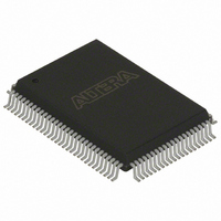
EPC16QI100 Altera, EPC16QI100 Datasheet - Page 29

EPC16QI100
Manufacturer Part Number
EPC16QI100
Description
IC CONFIG DEVICE 16MBIT 100-PQFP
Manufacturer
Altera
Series
EPCr
Datasheet
1.EPC8QC100.pdf
(34 pages)
Specifications of EPC16QI100
Programmable Type
In System Programmable
Memory Size
16Mb
Voltage - Supply
3 V ~ 3.6 V
Operating Temperature
-40°C ~ 85°C
Package / Case
100-MQFP, 100-PQFP
Lead Free Status / RoHS Status
Contains lead / RoHS non-compliant
Other names
544-1227
Available stocks
Company
Part Number
Manufacturer
Quantity
Price
Company:
Part Number:
EPC16QI100
Manufacturer:
ALTERA
Quantity:
58
Company:
Part Number:
EPC16QI100
Manufacturer:
LINEAR
Quantity:
200
Company:
Part Number:
EPC16QI100
Manufacturer:
ALTERA
Quantity:
2
Part Number:
EPC16QI100
Manufacturer:
ALTERA/阿尔特拉
Quantity:
20 000
Company:
Part Number:
EPC16QI100N
Manufacturer:
ALTERA
Quantity:
1 400
Company:
Part Number:
EPC16QI100N
Manufacturer:
Altera
Quantity:
135
Part Number:
EPC16QI100N
Manufacturer:
ALTERA/阿尔特拉
Quantity:
20 000
Chapter 1: Enhanced Configuration Devices (EPC4, EPC8, and EPC16) Data Sheet
Timing Information
Timing Information
Figure 1–7. Configuration Timing Waveform Using an Enhanced Configuration Device
Notes to
(1) The enhanced configuration device will drive DCLK low after configuration.
(2) The enhanced configuration device will drive DATA[] high after configuration.
Table 1–14. Enhanced Configuration Device Configuration Parameters (Part 1 of 2)
© December 2009 Altera Corporation
f
t
t
t
t
t
t
t
t
t
DCLK
DCLK
HC
LC
CE
OE
OH
CF
DF
RE
(2)
(2)
(3)
Symbol
Figure
nINIT_CONF or VCC/nCONFIG
f
1–7:
nCS/CONF_DONE
DCLK frequency
DCLK period
DCLK duty cycle high time
DCLK duty cycle low time
OE to first DCLK delay
OE to first DATA available
DCLK rising edge to DATA change
OE assert to DCLK disable delay
OE assert to DATA disable delay
DCLK rising edge to OE
OE/nSTATUS
INIT_DONE
DATA[7..0]
Figure 1–7
configuration device.
Table 1–14
devices.
For more information about the flash memory (external flash interface) timing, refer
to the appropriate flash data sheet on the Altera website at www.altera.com.
■
■
■
User I/O
DCLK
For Micron flash-based EPC4, refer to the Micron MT28F400B3 Data Sheet Flash
Memory Used in EPC4 Devices at
For Sharp flash-based EPC16, refer to the Sharp LHF16J06 Data Sheet Flash Memory
Used in EPC16 Devices at
For Intel flash-based EPC4 and EPC16, refer to Intel Flash 28F016B3 at
www.intel.com.
Parameter
t
OEZX
shows the configuration timing waveform when using an enhanced
defines the timing parameters when using the enhanced configuration
t
CO
Tri-State
t
t
Byte0 Byte1
POR
DSU
t
CL
Byte2 Byte3
t
DH
www.sharpsma.com.
t
CH
40% duty cycle
40% duty cycle
40% duty cycle
Condition
www.micron.com.
—
—
—
—
—
—
—
Byten
Tri-State
Configuration Handbook (Complete Two-Volume Set)
Min
277
277
(1)
—
15
60
40
40
6
6
Typ
—
—
—
—
—
—
—
—
—
—
User Mode
(2)
Max
66.7
—
—
—
—
—
—
—
—
—
MHz
Unit
ns
ns
ns
ns
ns
ns
ns
ns
ns
1–29


