EPCS1SI8 Altera, EPCS1SI8 Datasheet - Page 25
EPCS1SI8
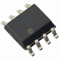
Manufacturer Part Number
EPCS1SI8
Description
IC CONFIG DEVICE 1MBIT 8-SOIC
Manufacturer
Altera
Series
EPCSr
Datasheet
1.EPCS1SI8.pdf
(38 pages)
Specifications of EPCS1SI8
Programmable Type
In System Programmable
Memory Size
1Mb
Voltage - Supply
3 V ~ 3.6 V
Operating Temperature
-40°C ~ 85°C
Package / Case
8-SOIC (0.154", 3.90mm Width)
Lead Free Status / RoHS Status
Contains lead / RoHS non-compliant
Other names
544-1241-5
Available stocks
Company
Part Number
Manufacturer
Quantity
Price
Company:

Part Number:
EPCS1SI8
Manufacturer:
ALTERA
Quantity:
22
Part Number:
EPCS1SI8
Manufacturer:
ALTERA/阿尔特拉
Quantity:
20 000
Company:
Part Number:
EPCS1SI8N
Manufacturer:
ALTERA
Quantity:
672


Chapter 3: Serial Configuration Devices (EPCS1, EPCS4, EPCS16, EPCS64, and EPCS128) Data Sheet
Serial Configuration Device Memory Access
Figure 3–17. Erase Sector Operation Timing Diagram
Note to
(1) Address bit A[23] is a don't-care bit in EPCS64. Address bits A[23..21] are don't-care bits in EPCS16. Address bits A[23..19] are don't-
© December 2009
care bits in EPCS4. Address bits A[23..17] are don't-care bits in EPCS1.
Figure
3–17:
Altera Corporation
You must account for this delay before accessing the memory contents. Alternatively,
you can check the write in progress bit in the status register by executing the read
status operation while the self-timed erase cycle is in progress. The write in progress
bit is 1 during the self-timed erase cycle and 0 when it is complete. The write enable
latch bit in the status register is reset to 0 before the erase cycle is complete.
Figure 3–16. Erase Bulk Operation Timing Diagram
Erase Sector Operation
The erase sector operation code is b'1101 1000, with the MSB listed first. The erase
sector operation allows the user to erase a certain sector in the serial configuration
device by setting all bits inside the sector to 1 or 0xFF. This operation is useful for
users who access the unused sectors as general purpose memory in their applications.
The write enable operation must be executed prior to the erase sector operation so
that the write enable latch bit in the status register is set to 1.
The erase sector operation is implemented by first driving nCS low, then shifting in
the erase sector operation code and the three address bytes of the chosen sector on the
ASDI pin. The three address bytes for the erase sector operation can be any address
inside the specified sector. (Refer to
range information.) Drive nCS high after the eighth bit of the erase sector operation
code has been latched in.
Immediately after the device drives nCS high, the self-timed erase sector cycle is
initiated. Refer to t
respective EPCS devices. You must account for this amount of delay before the
memory contents can be accessed. Alternatively, you can check the write in progress
bit in the status register by executing the read status operation while the erase cycle is
in progress. The write in progress bit is 1 during the self-timed erase cycle and 0 when
it is complete. The write enable latch bit in the status register resets to 0 before the
erase cycle is complete.
DCLK
ASDI
nCS
0
1
ES
2
Operation Code
in
3
DCLK
ASDI
nCS
Table 3–16
4
Figure 3–17
5
6
7
MSB
0
for the self-timed erase sector cycle time for the
23
Table 3–3
8
1
22
shows the timing diagram.
9
24-Bit Address (1)
2
Operation Code
3
4
through
Configuration Handbook (Complete Two-Volume Set)
3
28
5
2
29
6
1
30
7
Table 3–7
0
31
for sector address
3–25
Related parts for EPCS1SI8
Image
Part Number
Description
Manufacturer
Datasheet
Request
R

Part Number:
Description:
(EPCS1 - EPCS64) Serial Configuration Devices
Manufacturer:
Altera Corporation
Datasheet:

Part Number:
Description:
IC CONFIG DEVICE 1MBIT 8-DIP
Manufacturer:
Altera
Datasheet:

Part Number:
Description:
IC CONFIG DEVICE 1.6MBIT 20-PLCC
Manufacturer:
Altera
Datasheet:
Part Number:
Description:
IC CONFIG DEVICE 1.6MBIT 20-PLCC
Manufacturer:
Altera
Datasheet:

Part Number:
Description:
IC CONFIG DEVICE 1.6MBIT 32-TQFP
Manufacturer:
Altera
Datasheet:
Part Number:
Description:
IC CONFIG DEVICE 1.6MBIT 32-TQFP
Manufacturer:
Altera
Datasheet:
Part Number:
Description:
IC CONFIG DEVICE 1.6MBIT 20-PLCC
Manufacturer:
Altera
Datasheet:
Part Number:
Description:
IC CONFIG DEVICE 1.6MBIT 20-PLCC
Manufacturer:
Altera
Datasheet:

Part Number:
Description:
IC CONFIG DEVICE 8MBIT 100-PQFP
Manufacturer:
Altera
Datasheet:
Part Number:
Description:
IC CONFIG DEVICE 1.6MBIT 32-TQFP
Manufacturer:
Altera
Datasheet:
Part Number:
Description:
IC CONFIG DEVICE 1.6MBIT 32-TQFP
Manufacturer:
Altera
Datasheet:
Part Number:
Description:
IC CONFIG DEVICE 16MBIT 100-PQFP
Manufacturer:
Altera
Datasheet:
Part Number:
Description:
IC CONFIG DEVICE 16MBIT 100-PQFP
Manufacturer:
Altera
Datasheet:
Part Number:
Description:
IC CONFIG DEVICE 16MBIT 100-PQFP
Manufacturer:
Altera
Datasheet: