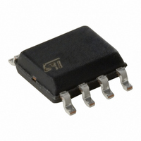
M24256-BWMN6P STMicroelectronics, M24256-BWMN6P Datasheet - Page 16

M24256-BWMN6P
Manufacturer Part Number
M24256-BWMN6P
Description
IC EEPROM 256KBIT 400KHZ 8SOIC
Manufacturer
STMicroelectronics
Datasheet
1.M24256-BWMN6TP.pdf
(42 pages)
Specifications of M24256-BWMN6P
Format - Memory
EEPROMs - Serial
Memory Type
EEPROM
Memory Size
256K (32K x 8)
Speed
400kHz
Interface
I²C, 2-Wire Serial
Voltage - Supply
2.5 V ~ 5.5 V
Operating Temperature
-40°C ~ 85°C
Package / Case
8-SOIC (3.9mm Width)
Lead Free Status / RoHS Status
Lead free / RoHS Compliant
Other names
497-8579-5
M24256-BWMN6P
M24256-BWMN6P
Available stocks
Company
Part Number
Manufacturer
Quantity
Price
Part Number:
M24256-BWMN6P
Manufacturer:
ST
Quantity:
20 000
Device operation
3.9
3.10
3.11
16/42
Write Identification Page (M24256-D only)
The Identification Page (64 bytes) is an additional page which can be written and (later)
permanently locked in Read-only mode. The identification page is written by issuing a Write
Identification Page instruction. This instruction uses the same protocol and format as Page
Write (into memory array), except for the following differences:
●
●
If the Identification page is locked, the data bytes transferred during the Write Identification
Page instruction are not acknowledged (NoAck).
Lock Identification Page (M24256-D only)
The Lock Identification Page instruction (Lock ID) permanently locks the Identification page
in read-only mode. The Lock ID instruction is similar to Byte Write (into memory array) with
the following specific conditions:
●
●
●
If the Identification Page is locked, the data bytes transferred during the ID Write instruction
are not acknowledged (NoAck).
ECC (error correction code) and write cycling
The M24256-Bx and M24256-D devices offer an ECC (error correction code) logic which
compares each 4-byte word with its six associated ECC EEPROM bits. As a result, if a
single bit out of 4 bytes of data happens to be erroneous during a Read operation, the ECC
detects it and replaces it by the correct value. The read reliability is therefore much improved
by the use of this feature.
Note however that even if a single byte has to be written, 4 bytes are internally modified
(plus the ECC bits), that is, the addressed byte is cycled together with the other three bytes
making up the word. It is therefore recommended to write data by word (4 bytes) at address
4*N (where N is an integer) in order to benefit from the larger amount of Write cycles.
The M24256-Bx and M24256-DR devices are qualified at 1 million (1 000 000) Write cycles,
using a cycling routine that writes to the device by multiples of 4-bytes.
Device Type Identifier = 1011b
MSB address bits A15/A6 are don't care except for address bit A10 which must be ‘0’.
LSB address bits A5/A0 define the byte address inside the identification page.
Device Type Identifier = 1011b
Address bit A10 must be ‘1’; all other address bits are don't care
The data byte must be equal to the binary value xxxx xx1x, where x is don't care.
Doc ID 6757 Rev 23
M24256-BF, M24256-BR, M24256-BW, M24256-DR


