CY7C1041CV33-12ZC Cypress Semiconductor Corp, CY7C1041CV33-12ZC Datasheet - Page 5
CY7C1041CV33-12ZC
Manufacturer Part Number
CY7C1041CV33-12ZC
Description
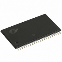
IC SRAM 4MBIT 12NS 44TSOP
Manufacturer
Cypress Semiconductor Corp
Datasheet
1.CY7C1041CV33-15VC.pdf
(12 pages)
Specifications of CY7C1041CV33-12ZC
Format - Memory
RAM
Memory Type
SRAM - Asynchronous
Memory Size
4M (256K x 16)
Speed
12ns
Interface
Parallel
Voltage - Supply
3 V ~ 3.6 V
Operating Temperature
0°C ~ 70°C
Package / Case
44-TSOP II
Lead Free Status / RoHS Status
Contains lead / RoHS non-compliant
Other names
428-1484
Available stocks
Company
Part Number
Manufacturer
Quantity
Price

Part Number:
CY7C1041CV33-12ZC
Manufacturer:
CYPRESS/赛普拉斯
Quantity:
20 000


Document #: 38-05134 Rev. *H
Thermal Resistance
AC Test Loads and Waveforms
AC Switching Characteristics
* CAPACITIVE LOAD CONSISTS
OF ALL COMPONENTS OF THE
TEST ENVIRONMENT
Parameter
Read Cycle
t
t
t
t
t
t
t
t
t
t
t
t
t
t
t
Notes:
power
RC
AA
OHA
ACE
DOE
LZOE
HZOE
LZCE
HZCE
PU
PD
DBE
LZBE
HZBE
4. AC characteristics (except High-Z) for 10-ns parts are tested using the load conditions shown in Figure (a). All other speeds are tested using the Thevenin load
5. Test conditions assume signal transition time of 3 ns or less, timing reference levels of 1.5V, input pulse levels of 0 to 3.0V.
6. t
7. t
8. At any given temperature and voltage condition, t
9. The internal Write time of the memory is defined by the overlap of CE LOW, and WE LOW. CE and WE must be LOW to initiate a Write, and the transition of
Parameter
10-ns Devices
shown in Figure (b). High-Z characteristics are tested for all speeds using the test load shown in Figure (d).
either of these signals can terminate the Write. The input data set-up and hold timing should be referenced to the leading edge of the signal that terminates the
Write.
Θ
Θ
POWER
HZOE
JA
JC
[6]
GND
3.0V
OUTPUT
, t
Rise Time: 1 V/ns
HZCE
gives the minimum amount of time that the power supply should be at typical V
Thermal Resistance (Junction to Ambient) Test conditions follow standard
Thermal Resistance (Junction to Case)
, and t
V
Read Cycle Time
Address to Data Valid
Data Hold from Address Change
CE LOW to Data Valid
OE LOW to Data Valid
OE LOW to Low-Z
OE HIGH to High-Z
CE LOW to Low-Z
CE HIGH to High-Z
CE LOW to Power-Up
CE HIGH to Power-Down
Byte Enable to Data Valid
Byte Enable to Low-Z
Byte Disable to High-Z
CC
HZWE
(typical) to the first access
are specified with a load capacitance of 5 pF as in part (d) of AC Test Loads. Transition is measured ±500 mV from steady-state voltage
10%
Z = 50Ω
Description
[3]
90%
Description
ALL INPUT PULSES
[8]
(a)
[7, 8]
[7, 8]
1.5V
50 Ω
(c)
[5]
[4]
Over the Operating Range
HZCE
is less than t
30 pF*
Fall Time: 1 V/ns
Min.
100
90%
10
3
0
3
0
0
10%
-10
test methods and procedures for
measuring thermal impedance,
per EIA / JESD51.
LZCE
12-, 15-, 20-ns Devices
Max.
10
10
10
, t
5
5
5
5
6
OUTPUT
HZOE
Test Conditions
3.3V
is less than t
Min.
100
12
3
0
3
0
0
CC
30 pF
-12
(b)
values until the first memory access can be performed.
LZOE
Max.
12
12
12
6
6
6
6
6
, and t
R 317Ω
HZWE
Min.
100
15
3
0
3
0
0
is less than t
High-Z Characteristics
351Ω
-15
TSOP-II
R2
42.96
10.75
OUTPUT
Max.
15
15
15
7
7
7
7
7
3.3V
LZWE
CY7C1041CV33
(d)
FBGA
Min.
38.15
for any given device.
100
9.15
20
3
0
3
0
0
5 pF
-20
Max.
R 317Ω
20
20
20
25.99
8
8
8
8
8
SOJ
18.8
Page 5 of 12
Unit
351Ω
°C/W
°C/W
µs
ns
ns
ns
ns
ns
ns
ns
ns
ns
ns
ns
ns
ns
ns
Unit
R2
Related parts for CY7C1041CV33-12ZC
Image
Part Number
Description
Manufacturer
Datasheet
Request
R

Part Number:
Description:
Manufacturer:
Cypress Semiconductor Corp
Datasheet:
Part Number:
Description:
Manufacturer:
Cypress Semiconductor Corp
Datasheet:
Part Number:
Description:
Manufacturer:
Cypress Semiconductor Corp
Datasheet:
Part Number:
Description:
Manufacturer:
Cypress Semiconductor Corp
Datasheet:
Part Number:
Description:
Manufacturer:
Cypress Semiconductor Corp
Datasheet: