CY7C1021CV33-12VC Cypress Semiconductor Corp, CY7C1021CV33-12VC Datasheet - Page 3
CY7C1021CV33-12VC
Manufacturer Part Number
CY7C1021CV33-12VC
Description
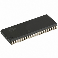
IC SRAM 1MBIT 12NS 44SOJ
Manufacturer
Cypress Semiconductor Corp
Datasheet
1.CY7C1021CV33-10VC.pdf
(12 pages)
Specifications of CY7C1021CV33-12VC
Format - Memory
RAM
Memory Type
SRAM - Asynchronous
Memory Size
1M (64K x 16)
Speed
12ns
Interface
Parallel
Voltage - Supply
3 V ~ 3.6 V
Operating Temperature
0°C ~ 70°C
Package / Case
44-SOJ
Lead Free Status / RoHS Status
Contains lead / RoHS non-compliant
Other names
428-1480


Document #: 38-05132 Rev. *C
Maximum Ratings
(Above which the useful life may be impaired. For user guide-
lines, not tested.)
Storage Temperature .................................–65 C to +150 C
Ambient Temperature with
Power Applied............................................. –55 C to +125 C
Supply Voltage on V
DC Voltage Applied to Outputs
in High-Z State
DC Input Voltage
Electrical Characteristics
Capacitance
V
V
V
V
I
I
I
I
I
I
C
C
Notes:
Parameter
IX
OZ
OS
CC
SB1
SB2
1.
2.
3.
OH
OL
IH
IL
IN
OUT
V
Not more than one output should be shorted at one time. Duration of the short circuit should not exceed 30 seconds.
Tested initially and after any design or process changes that may affect these parameters.
IL
Parameter
(min.) = –2.0V for pulse durations of less than 20 ns.
Output HIGH
Voltage
Output LOW
Voltage
Input HIGH Voltage
Input LOW
Voltage
Input Load Current GND < V
Output Leakage
Current
Output Short Circuit
Current
V
Supply Current
Automatic CE
Power-Down
Current —TTL
Inputs
Automatic CE
Power-Down
Current —CMOS
Inputs
CC
[1]
[3]
Description
[1]
......................................–0.5V to V
Operating
...................................–0.5V to V
CC
[1]
[2]
to Relative GND
Input Capacitance
Output Capacitance
Description
Over the Operating Range
V
I
V
I
GND < V
Output Disabled
V
V
V
I
f = f
Max. V
V
V
f = f
Max. V
CE > V
V
or V
OH
OL
OUT
CC
CC
CC
OUT
CC
IN
IN
CC
= 8.0 mA
MAX
MAX
= –4.0 mA
> V
< V
IN
= Min.,
= Min.,
= Max.,
= Max.,
– 0.3V,
= 0 mA,
Conditions
[1]
= GND
< 0.3V, f = 0
CC
CC
CC
IH
IL
= 1/t
.... –0.5V to +4.6V
,
Test
I
I
, CE > V
,
or
– 0.3V, V
< V
< V
RC
CC
CC
,
CC
CC
IH
IN
+0.5V
+0.5V
>
T
V
A
CC
1021CV33-8
= 25 C, f = 1 MHz,
Min.
–0.3
2.4
2.0
= 3.3V
1
1
Test Conditions
Current into Outputs (LOW)......................................... 20 mA
Static Discharge Voltage............................................ >2001V
(per MIL-STD-883, Method 3015)
Latch-up Current...................................................... >200 mA
Operating Range
Max.
+ 0.3
-300
V
Commercial
Industrial
0.4
0.8
95
15
CC
5
1
1
Range
1021CV33-10 1021CV33-12 1021CV33-15
Min.
2.4
2.0
0.3
1
1
Max.
+ 0.3
V
0.4
0.8
+1
+1
300
90
15
CC
5
Ambient Temperature
–40 C to +85 C
0 C to +70 C
Min.
–0.3
2.4
2.0
–1
–1
Max.
Max.
+ 0.3
–300
V
0.4
0.8
8
8
+1
+1
85
15
CY7C1021CV33
CC
5
Min.
–0.3
2.4
2.0
–1
–1
3.3V
3.3V
Page 3 of 12
Max.
+ 0.3
–300
V
0.4
0.8
Unit
+1
+1
80
15
V
5
CC
pF
pF
CC
10%
10%
Unit
mA
mA
mA
mA
V
V
V
V
A
A
Related parts for CY7C1021CV33-12VC
Image
Part Number
Description
Manufacturer
Datasheet
Request
R

Part Number:
Description:
Manufacturer:
Cypress Semiconductor Corp
Datasheet:
Part Number:
Description:
Manufacturer:
Cypress Semiconductor Corp
Datasheet:
Part Number:
Description:
Manufacturer:
Cypress Semiconductor Corp
Datasheet:
Part Number:
Description:
Manufacturer:
Cypress Semiconductor Corp
Datasheet:
Part Number:
Description:
Manufacturer:
Cypress Semiconductor Corp
Datasheet: