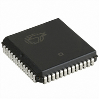
CY7C141-25JC Cypress Semiconductor Corp, CY7C141-25JC Datasheet

CY7C141-25JC
Specifications of CY7C141-25JC
Available stocks
Related parts for CY7C141-25JC
CY7C141-25JC Summary of contents
Page 1
... An automatic power-down feature is controlled independently on each port by the chip enable (CE) pins. The CY7C130 and CY7C140 are available in 48-pin DIP. The CY7C131 and CY7C141 are available in 52-pin PLCC and PQFP. I/O CONTROL MEMORY ...
Page 2
... Static Discharge Voltage .......................................... >2001V (per MIL-STD-883, Method 3015) Latch-Up Current .................................................... >200 mA Operating Range Range Commercial Industrial [5] Military 2 CY7C130/CY7C131 CY7C140/CY7C141 PQFP Top View 52 5150 7C131 33 7C141 1415 C130-4 7C130-35 7C130-45 7C131-35 7C131-45 7C140-35 ...
Page 3
... CC Mil > V – 0.2V CC < 0.2V, IN [10] and using AC Test Waveforms input levels of GND to 3V. RC Test Conditions MHz 5. CY7C130/CY7C131 CY7C140/CY7C141 [3] 7C130-30 7C130-35 7C130-45,55 7C131-25,30 7C131-35 7C131-45,55 7C140-30 7C140-35 7C140-45,55 7C141-25,30 7C141-35 7C141-45,55 Min. Max. Min. Max. Min. Max. Unit 2.4 2.4 2 ...
Page 4
... HZCE LZCE = 5pF as in part ( Test Loads . Transition is measured ±500 mV from steady state voltage CY7C130/CY7C131 CY7C140/CY7C141 BUSY OR INT BUSY Output Load ALL INPUT PULSES (CY7C130/CY7C131 ONLY) 90% 90% 10% 5ns [3] 7C130-25 7C130-30 7C131-25 7C131-30 [3,4] 7C140-25 7C140-30 7C141-25 7C141-30 Max ...
Page 5
... These parameters are measured from the input signal changing, until the output pin goes to a high-impedance state. 17. CY7C140/CY7C141 only. 18. A write operation on Port A, where Port A has priority, leaves the data on Port B’s outputs undisturbed until one access time after one of the following: BUSY on Port B goes HIGH. Port B’ ...
Page 6
... R/W is HIGH for read cycle. 20. Device is continuously selected and [6,11] (continued) 7C130-35 7C131-35 7C140-35 7C141-35 Min. Max [16 [16 Note 18 Note [16] 25 [16] 25 [16] 25 Either Port Address Access CY7C130/CY7C131 CY7C140/CY7C141 7C130-45 7C130-55 7C131-45 7C131-55 7C140-45 7C140-55 7C141-45 7C141-55 Min. Max. Min. Max. Unit ...
Page 7
... ADDRESS MATCH t PWE ADDRESS MATCH BLA [15, 22] Either Port SCE PWE t SD DATA VALID HIGH IMPEDANCE or t PWE HZWE 7 CY7C130/CY7C131 CY7C140/CY7C141 t HZCE t HZOE DATA VALID VALID t BHA t BDD t DDD t WDD allow the data I/O pins to enter high impedance and for data SD C130-8 ...
Page 8
... If the CE LOW transition occurs simultaneously with or after the R/W LOW transition, the outputs remain in the high-impedance state [16, 23] Either Port SCE PWE t SD DATA VALID t HZWE HIGH IMPEDANCE ADDRESS MATCH BLC ADDRESS MATCH BLC 8 CY7C130/CY7C131 CY7C140/CY7C141 LZWE C130-11 BHC C130-12 BHC C130-13 ...
Page 9
... Busy Timing Diagram No. 2 (Address Arbitration) Left Address Valid First: ADDRESS MATCH ADDRESS ADDRESS R BUSY R Right Address Valid First: ADDRESS MATCH ADDRESS ADDRESS L BUSY L Busy Timing Diagram No. 3 Write with BUSY (Slave:CY7C140/CY7C141 BUSY ADDRESS MISMATCH t t BLA BHA ADDRESS MISMATCH t t ...
Page 10
... Right Side Sets INT L ADDR R t INS INT L Left Side Clears INT L ADDR R INT WRITE 3FF EINS t WINS EINR t WC WRITE 3FE EINS t WINS EINR 10 CY7C130/CY7C131 CY7C140/CY7C141 t RC READ 3FF t INT t OINR C130- READ 3FE t INR t OINR C130-17 C130-18 C130-20 ...
Page 11
... TYPICAL ACCESS TIME CHANGE vs. OUTPUT LOADING 30.0 25.0 20.0 15.0 10.0 V =4.5V CC 5 5.0 0 200 400 600 800 CAPACITANCE (pF) 11 CY7C130/CY7C131 CY7C140/CY7C141 OUTPUT SOURCE CURRENT vs. OUTPUT VOLTAGE 120 100 =5. = 125 0 1.0 2.0 3.0 OUTPUT VOLTAGE (V) OUTPUT SINK CURRENT vs.OUTPUT VOLTAGE 140 ...
Page 12
... N52 52-Pin Plastic Quad Flatpack J69 52-Lead Plastic Leaded Chip Carrier N52 52-Pin Plastic Quad Flatpack J69 52-Lead Plastic Leaded Chip Carrier N52 52-Pin Plastic Quad Flatpack 12 CY7C130/CY7C131 CY7C140/CY7C141 Operating Range Commercial Industrial Commercial Industrial Military Commercial Industrial Military Commercial Industrial ...
Page 13
... CY7C140-30PC CY7C140-30PI 35 CY7C140-35PC CY7C140-35PI CY7C140-35DMB 45 CY7C140-45PC CY7C140-45PI CY7C140-45DMB 55 CY7C140-55PC CY7C140-55PI CY7C140-55DMB Speed Package (ns) Ordering Code 15 CY7C141-15JC CY7C141-15NC 25 CY7C141-25JC CY7C141-25NC CY7C141-25JI CY7C141-25NI 30 CY7C141-30JC CY7C141-30NC CY7C141-30JI 35 CY7C141-35JC CY7C141-35NC CY7C141-35JI CY7C141-35NI 45 CY7C141-45JC CY7C141-45NC CY7C141-45JI CY7C141-45NI 55 CY7C141-55JC CY7C141-55NC CY7C141-55JI CY7C141-55NI Shaded area contains preliminary information. ...
Page 14
... WRITE CYCLE 10 10, 11 SCE 10, 11 PWE 10 10 Parameter Subgroups BUSY/INTERRUPT TIMING 10, 11 BLA 10, 11 BHA 10, 11 BLC 10, 11 BHC 10 10, 11 WINS 10, 11 EINS 10, 11 INS 10, 11 OINR 10, 11 EINR 10, 11 INR BUSY TIMING [ 10, 11 BDD Note: 24. CY7C140/CY7C141 only. Document #: 38-00027 ...
Page 15
... Package Diagrams 48-Lead (600-Mil) Sidebraze DIP D26 52-Lead Plastic Leaded Chip Carrier J69 15 CY7C130/CY7C131 CY7C140/CY7C141 ...
Page 16
... The inclusion of Cypress Semiconductor products in life-support systems application implies that the manufacturer assumes all risk of such use and in doing so indemnifies Cypress Semiconductor against all charges. 48-Lead (600-Mil) Molded DIP P25 CY7C130/CY7C131 CY7C140/CY7C141 ...


