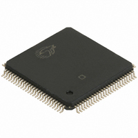
CY7C025AV-20AC Cypress Semiconductor Corp, CY7C025AV-20AC Datasheet

CY7C025AV-20AC
Specifications of CY7C025AV-20AC
Available stocks
Related parts for CY7C025AV-20AC
CY7C025AV-20AC Summary of contents
Page 1
... BUSY is an output in master mode and an input in slave mode. Cypress Semiconductor Corporation Document #: 38-06052 Rev. *B • Automatic power-down • Expandable data bus to 32/36 bits or more using Master/Slave chip select when using more than one device • On-chip arbitration logic • ...
Page 2
... I/O 13L 8 GND 9 I/O 10 14L I/O 11 15L GND Notes the CY7C025AV. 12L the CY7C025AV. 12R Document #: 38-06052 Rev. *B 100-Pin TQFP Top View 100 CY7C024AV (4K × 16) CY7C025AV (8K × 16 CY7C024AV/025AV/026AV CY7C0241AV/0251AV/036AV INT 65 L BUSY 64 L GND 63 M/S 62 BUSY 61 R INT ...
Page 3
Pin Configurations (continued) 100 I I/O 4 17L I/O 11L 5 I/O 6 12L I/O 13L 7 I/O 14L 8 GND 9 I/O 10 15L I/O 11 16L GND ...
Page 4
Pin Configurations (continued I/O 8L I/O 17L I/O 11L I/O 12L I/O 13L I/O 14L GND I/O 15L I/O 16L V CC GND I/O 0R I I/O 3R I/O 4R I/O 5R I/O ...
Page 5
... Two ports are provided, permitting independent, asynchronous access for reads and writes to any location in memory. The devices can be utilized as standalone 16/18-bit dual-port static RAMs or multiple devices can be combined in order to function as a 32/36-bit or wider master/slave dual-port static RAM ...
Page 6
... CY7C026AV/36AV) is the mailbox for the right port and the second-highest memory location (FFE for the CY7C024AV/ 41AV, 1FFE for the CY7C025AV/51AV, 3FFE for the CY7C026AV/36AV) is the mailbox for the left port. When one port writes to the other port’s mailbox, an interrupt is generated to the owner ...
Page 7
... Left port writes 1 to semaphore Right port writes 0 to semaphore Right port writes 1 to semaphore Left port writes 0 to semaphore Left port writes 1 to semaphore Notes: 9. See Functional Description for specific highest memory locations by device. 10. If BUSY =L, then no change. R 11. If BUSY =L, then no change ...
Page 8
Maximum Ratings (Above which the useful life may be impaired. For user guide- lines, not tested.) Storage Temperature .................................– +150 C Ambient Temperature with Power Applied.............................................– +125 C Supply Voltage to Ground Potential ............... –0.5V ...
Page 9
AC Test Loads and Waveforms 3. 590 OUTPUT 435 (a) Normal Load (Load 1) Switching Characteristics Over the Operating Range Parameter Read Cycle t Read Cycle Time RC t Address to Data ...
Page 10
Switching Characteristics Over the Operating Range Parameter t Data Hold From Write End HD [21, 22] t R/W LOW to High Z HZWE [21, 22] t R/W HIGH to Low Z LZWE [23] t Write Pulse to Data Delay WDD ...
Page 11
Switching Waveforms Read Cycle No.1 (Either Port Address Access) ADDRESS t OHA DATA OUT PREVIOUS DATA VALID Read Cycle No.2 (Either Port CE/OE Access) CE and DATA OUT I CC CURRENT I SB [27, 29, 30, ...
Page 12
Switching Waveforms (continued) Write Cycle No.1: R/W Controlled Timing ADDRESS OE [36, 37 R/W NOTE 39 DATA OUT DATA IN Write Cycle No Controlled Timing ADDRESS [36, 37 R/W DATA IN Notes: ...
Page 13
Switching Waveforms (continued) Semaphore Read After Write Timing, Either Side A –A VALID ADRESS 0 2 SEM I R/W OE Timing Diagram of Semaphore Contention A – R/W L SEM L A – ...
Page 14
Switching Waveforms (continued) Timing Diagram of Read with BUSY (M/S=HIGH) ADDRESS R R/W R DATA ADDRESS L BUSY L DATA OUTL Write Timing with Busy Input (M/S=LOW) R/W BUSY Note: 45 LOW. ...
Page 15
Switching Waveforms (continued) Busy Timing Diagram No.1 (CE Arbitration) CE Valid First: L ADDRESS L BUSY R CE ValidFirst: R ADDRESS L BUSY L Busy Timing Diagram No.2 (Address Arbitration) Left Address ...
Page 16
Switching Waveforms (continued) Interrupt Timing Diagrams Left Side Sets INT R : ADDRESS WRITE 1FFF (OR 1/3FFF R/W L INT R t INS Right Side Clears INT R : ADDRESS R ...
Page 17
... Ordering Information 4K x16 3.3V Asynchronous Dual-Port SRAM Speed (ns) Ordering Code 20 CY7C024AV-20AC 25 CY7C024AV-25AC 8K x16 3.3V Asynchronous Dual-Port SRAM Speed (ns) Ordering Code 20 CY7C025AV-20AC 25 CY7C025AV-25AC CY7C025AV-25AI 16K x18 3.3V Asynchronous Dual-Port SRAM Speed (ns) Ordering Code 20 CY7C026AV-20AC 25 CY7C026AV-25AC CY7C026AV-25AI 4K x18 3.3V Asynchronous Dual-Port SRAM Speed ...
Page 18
... Document #: 38-06052 Rev. *B © Cypress Semiconductor Corporation, 2003. The information contained herein is subject to change without notice. Cypress Semiconductor Corporation assumes no responsibility for the use of any circuitry other than circuitry embodied in a Cypress Semiconductor product. Nor does it convey or imply any license under patent or other rights. Cypress Semiconductor does not authorize its products for use as critical components in life-support systems where a malfunction or failure may reasonably be expected to result in significant injury to the user ...
Page 19
... Document History Page Document Title: CY7C024AV/CY7C025AV/CY7C026AV/CY7C0241AV/CY7C0251AV/CY7C036AV 3.3V 4K/8K/16K x 16/18 Dual Port Static RAM Document Number: 38-06052 REV. ECN NO. Issue Date ** 110204 11/11/01 *A 122302 12/27/02 *B 128958 9/03/03 Document #: 38-06052 Rev. *B Orig. of Change SZV Change from Spec number: 38-00838 to 38-06052 RBI Power up requirements added to Maximum Ratings Information ...


