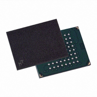
MT28F128J3FS-12 MET Micron Technology Inc, MT28F128J3FS-12 MET Datasheet - Page 28

MT28F128J3FS-12 MET
Manufacturer Part Number
MT28F128J3FS-12 MET
Description
IC FLASH 128MBIT 120NS 64FBGA
Manufacturer
Micron Technology Inc
Datasheet
1.MT28F128J3FS-12_ET_TR.pdf
(55 pages)
Specifications of MT28F128J3FS-12 MET
Format - Memory
FLASH
Memory Type
FLASH
Memory Size
128M (16Mx8, 8Mx16)
Speed
120ns
Interface
Parallel
Voltage - Supply
2.7 V ~ 3.6 V
Operating Temperature
-40°C ~ 85°C
Package / Case
64-FBGA
Lead Free Status / RoHS Status
Contains lead / RoHS non-compliant
Table 19: Configuration Coding Definitions
NOTE:
SET BLOCK LOCK BITS Command
enabled via a combination of block lock bits. The block
lock bits gate PROGRAM and ERASE operations. Using
the SET BLOCK LOCK BITS command, individual
block lock bits can be set. This command is invalid
when the ISM is running or when the device is sus-
pended. SET BLOCK LOCK BITS commands are exe-
cuted by a two-cycle sequence. The set block lock bits
setup, along with appropriate block address, is fol-
lowed by the set block lock bits confirm and an
address within the block to be locked. The ISM then
controls the set lock bit algorithm. When the sequence
is written, the device automatically outputs status reg-
ister data when read (see Figure 14 on page 36). The
CPU can detect the completion of the set block lock bit
event by analyzing the STS pin output or status register
bit SR7. Upon completion of set block lock bits opera-
tion, status register bit SR4 should be checked for
error. If an error is detected, the status register should
be cleared. The CEL remains in read status register
mode until a new command is issued. This two-step
sequence of setup followed by execution ensures that
lock bits are not accidentally set. An invalid SET
BLOCK LOCK BITS command results in status register
bits SR4 and SR5 being set to “1.”
09005aef80b5a323
MT28F640J3.fm – Rev. N 3/05 EN
DQ1–DQ0 = STS Configuration Codes
00 = Default, RY/BY# level mode (device
ready) indication
01 = Pulse on Erase Complete
10 = Pulse on Program Complete
11 = Pulse on Erase or Program Complete
1. An invalid configuration code will result in both SR4 and SR5 being set.
2. When the device is configured in one of the pulse modes, the STS pin pulses LOW with a typical pulse width of
A flexible block locking and unlocking scheme is
250ns.
DQ7
DQ6
DQ5
RESERVED
Used to generate a system interrupt pulse when any Flash device is an array
Used to generate system interrupts to trigger enabling of Flash arrays when
Used to control HOLD to a memory controller to prevent accessing a Flash
memory subsystem while any Flash device’s ISM is busy.
has completed a BLOCK ERASE or sequence of queued BLOCK ERASEs;
helpful for reformatting blocks after file system free space reclamation or
“clean-up.”
Used to generate a system interrupt pulse when any Flash device in an array
has completed a PROGRAM operation. Provides highest performance for
enabling continuous BUFFER WRITE operations.
either ERASE or PROGRAM operations are completed and a common
interrupt service routine is desired.
DQ4
28
CLEAR BLOCK LOCK BITS Command
all set block lock bits in parallel. This command is
invalid when the ISM is running or the device is sus-
pended. The CLEAR BLOCK LOCK BITS command is
executed by a two-cycle sequence. First, a clear block
lock bits setup is written, followed by a CLEAR BLOCK
LOCK BITS CONFIRM command. Then the device
automatically outputs status register data when read
(see Figure 14 on page 36). The CPU can detect com-
pletion of the clear block lock bits event by analyzing
the STS pin output or the status register bit SR7. When
the operation is completed, status register bit SR5
should be checked. If a clear block lock bits error is
detected, the status register should be cleared. The
CEL remains in read status register mode until another
command is issued.
lock bits are not accidentally cleared. An invalid
CLEAR BLOCK LOCK BITS command sequence results
in status register bits SR4 and SR5 being set to “1.”
Also, a reliable CLEAR BLOCK LOCK BITS operation
can only occur when V
block lock bits operation is attempted when V
V
LOCK BITS operation is aborted due to V
transitioning out of valid range, block lock bit values
1
PENLK
DQ3
The CLEAR BLOCK LOCK BITS command can clear
This two-step setup sequence ensures that block
Micron Technology, Inc., reserves the right to change products or specifications without notice.
, SR3 and SR5 are set to “1.” If a CLEAR BLOCK
NOTES
DQ2
128Mb, 64Mb, 32Mb
Q-FLASH MEMORY
CC
and V
COMPLETE
PROGRAM
PULSE ON
DQ1
PEN
are valid. If a clear
2
©2000 Micron Technology. Inc.
COMPLETE
PULSE ON
PEN
ERASE
DQ0
or V
PEN
CC
2
≤


