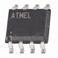
AT45DB041D-SSU Atmel, AT45DB041D-SSU Datasheet - Page 33

AT45DB041D-SSU
Manufacturer Part Number
AT45DB041D-SSU
Description
IC FLASH 4MBIT 66MHZ 8SOIC
Manufacturer
Atmel
Specifications of AT45DB041D-SSU
Format - Memory
FLASH
Memory Type
DataFLASH
Memory Size
4M (2048 pages x 264 bytes)
Speed
66MHz
Interface
SPI, RapidS
Voltage - Supply
2.7 V ~ 3.6 V
Operating Temperature
-40°C ~ 85°C
Package / Case
8-SOIC (3.9mm Width)
Density
4Mb
Access Time (max)
6ns
Interface Type
Serial (SPI)
Boot Type
Not Required
Address Bus
1b
Operating Supply Voltage (typ)
3/3.3V
Operating Temp Range
-40C to 85C
Package Type
SOIC
Program/erase Volt (typ)
2.7 to 3.6V
Sync/async
Synchronous
Operating Temperature Classification
Industrial
Operating Supply Voltage (min)
2.7V
Operating Supply Voltage (max)
3.6V
Supply Current
15mA
Mounting
Surface Mount
Pin Count
8
Architecture
Sectored
Supply Voltage (max)
3.6 V
Supply Voltage (min)
2.7 V
Maximum Operating Current
15 mA
Mounting Style
SMD/SMT
Organization
64 KB x 8
Memory Configuration
2048 Pages X 256 Bytes
Clock Frequency
50MHz
Supply Voltage Range
2.7V To 3.6V
Memory Case Style
SOIC
Rohs Compliant
Yes
Lead Free Status / RoHS Status
Lead free / RoHS Compliant
Available stocks
Company
Part Number
Manufacturer
Quantity
Price
Company:
Part Number:
AT45DB041D-SSU
Manufacturer:
ATMEL
Quantity:
12 000
Part Number:
AT45DB041D-SSU
Manufacturer:
ATMEL/爱特梅尔
Quantity:
20 000
Part Number:
AT45DB041D-SSU-2.5
Manufacturer:
ATMEL/爱特梅尔
Quantity:
20 000
18. Electrical Specifications
Table 18-1.
Table 18-2.
Table 18-3.
Notes:
3595J–DFLASH–08/07
Temperature under Bias ................................ -55°C to +125°C
Storage Temperature ..................................... -65°C to +150°C
All Input Voltages (including NC Pins)
with Respect to Ground ...................................-0.6V to +6.25V
All Output Voltages
with Respect to Ground .............................-0.6V to V
Operating Temperature (Case)
V
Symbol
I
I
I
I
I
I
V
V
V
V
DP
SB
CC1
CC2
LI
LO
CC
IL
IH
OL
OH
(1)
Power Supply
1. I
2. All inputs are 5 volts tolerant.
CC1
Parameter
Deep Power-down Current
Standby Current
Active Current, Read Operation
Active Current, Program/Erase
Operation
Input Load Current
Output Leakage Current
Input Low Voltage
Input High Voltage
Output Low Voltage
Output High Voltage
Absolute Maximum Ratings*
DC and AC Operating Range
DC Characteristics
during a buffer read is 20 mA maximum @ 20 MHz.
Ind.
Condition
CS, RESET, WP = V
inputs at CMOS levels
CS, RESET, WP = V
inputs at CMOS levels
f = 20 MHz; I
V
f = 33 MHz; I
V
f = 50 MHz; I
V
f = 66 MHz; I
V
V
V
V
I
I
OL
OH
CC
CC
CC
CC
CC
IN
I/O
= 1.6 mA; V
= -100 µA
= CMOS levels
= CMOS levels
= 3.6V
= 3.6V
= 3.6V
= 3.6V
= 3.6V
CC
+ 0.6V
OUT
OUT
OUT
OUT
CC
= 0 mA;
= 0 mA;
= 0 mA;
= 0 mA;
AT45DB041D (2.5V Version)
= 2.7V
IH
IH
, all
, all
*NOTICE:
-40°C to 85°C
2.5V to 3.6V
V
V
CC
CC
Stresses beyond those listed under “Absolute
Maximum Ratings” may cause permanent dam-
age to the device. This is a stress rating only and
functional operation of the device at these or any
other conditions beyond those indicated in the
operational sections of this specification is not
implied. Exposure to absolute maximum rating
conditions for extended periods may affect device
reliability.
Min
- 0.2V
x 0.7
Typ
25
10
11
12
5
7
8
AT45DB041D
AT45DB041D
-40°C to 85°C
V
2.7V to 3.6V
CC
Max
0.4
10
50
10
12
14
15
17
1
1
x 0.3
Units
mA
mA
mA
mA
mA
µA
µA
µA
µA
V
V
V
V
33


