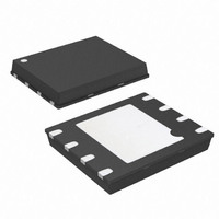
AT45DB081D-MU Atmel, AT45DB081D-MU Datasheet - Page 6

AT45DB081D-MU
Manufacturer Part Number
AT45DB081D-MU
Description
IC FLASH 8MBIT 66MHZ 8VDFN
Manufacturer
Atmel
Datasheet
1.AT45DB081D-MU.pdf
(53 pages)
Specifications of AT45DB081D-MU
Format - Memory
FLASH
Memory Type
DataFLASH
Memory Size
8M (4096 pages x 264 bytes)
Speed
66MHz
Interface
SPI, RapidS
Voltage - Supply
2.7 V ~ 3.6 V
Operating Temperature
-40°C ~ 85°C
Package / Case
8-VFQFN, 8-VFQFPN
Architecture
Sectored
Interface Type
SPI
Supply Voltage (max)
3.6 V
Supply Voltage (min)
2.7 V
Maximum Operating Current
15 mA
Mounting Style
SMD/SMT
Organization
64 KB x 16
Density
8Mb
Access Time (max)
6ns
Boot Type
Not Required
Address Bus
1b
Operating Supply Voltage (typ)
3/3.3V
Operating Temp Range
-40C to 85C
Package Type
MLF EP
Program/erase Volt (typ)
2.7 to 3.6V
Sync/async
Synchronous
Operating Temperature Classification
Industrial
Operating Supply Voltage (min)
2.7V
Operating Supply Voltage (max)
3.6V
Supply Current
15mA
Mounting
Surface Mount
Pin Count
8
Lead Free Status / RoHS Status
Lead free / RoHS Compliant
Available stocks
Company
Part Number
Manufacturer
Quantity
Price
Part Number:
AT45DB081D-MU
Manufacturer:
ATMEL/爱特梅尔
Quantity:
20 000
6.2
6.3
6
Continuous Array Read (High Frequency Mode: 0BH): Up to 66MHz
Continuous Array Read (Low Frequency Mode: 03H): Up to 33MHz
Atmel AT45DB081D
Continuous Array Read, the device will continue reading at the beginning of the next page with
no delays incurred during the page boundary crossover (the crossover from the end of one page
to the beginning of the next page). When the last bit in the main memory array has been read,
the device will continue reading back at the beginning of the first page of memory. As with cross-
ing over page boundaries, no delays will be incurred when wrapping around from the end of the
array to the beginning of the array.
A low-to-high transition on the CS pin will terminate the read operation and tri-state the output
pin (SO). The maximum SCK frequency allowable for the Continuous Array Read is defined by
the f
contents of the buffers unchanged.
This command can be used with the serial interface to read the main memory array sequentially
in high speed mode for any clock frequency up to the maximum specified by f
continuous read array with the page size set to 264-bytes, the CS must first be asserted then an
opcode 0BH must be clocked into the device followed by three address bytes and a dummy
byte. The first 12 bits (PA11 - PA0) of the 21-bit address sequence specify which page of the
main memory array to read, and the last nine bits (BA8 - BA0) of the 21-bit address sequence
specify the starting byte address within the page. To perform a continuous read with the page
size set to 256-bytes, the opcode, 0BH, must be clocked into the device followed by three
address bytes (A19 - A0) and a dummy byte. Following the dummy byte, additional clock pulses
on the SCK pin will result in data being output on the SO (serial output) pin.
The CS pin must remain low during the loading of the opcode, the address bytes, and the read-
ing of data. When the end of a page in the main memory is reached during a Continuous Array
Read, the device will continue reading at the beginning of the next page with no delays incurred
during the page boundary crossover (the crossover from the end of one page to the beginning of
the next page). When the last bit in the main memory array has been read, the device will con-
tinue reading back at the beginning of the first page of memory. As with crossing over page
boundaries, no delays will be incurred when wrapping around from the end of the array to the
beginning of the array. A low-to-high transition on the CS pin will terminate the read operation
and tri-state the output pin (SO). The maximum SCK frequency allowable for the Continuous
Array Read is defined by the f
data buffers and leaves the contents of the buffers unchanged.
This command can be used with the serial interface to read the main memory array sequentially
without a dummy byte up to maximum frequencies specified by f
read array with the page size set to 264-bytes, the CS must first be asserted then an opcode,
03H, must be clocked into the device followed by three address bytes (which comprise the 24-bit
page and byte address sequence). The first 12 bits (PA11 - PA0) of the 21-bit address sequence
specify which page of the main memory array to read, and the last nine bits (BA8 - BA0) of the
21-bit address sequence specify the starting byte address within the page. To perform a contin-
uous read with the page size set to 256-bytes, the opcode, 03H, must be clocked into the device
followed by three address bytes (A19 - A0). Following the address bytes, additional clock pulses
on the SCK pin will result in data being output on the SO (serial output) pin.
The CS pin must remain low during the loading of the opcode, the address bytes, and the read-
ing of data. When the end of a page in the main memory is reached during a Continuous Array
Read, the device will continue reading at the beginning of the next page with no delays incurred
CAR1
specification. The Continuous Array Read bypasses both data buffers and leaves the
CAR1
specification. The Continuous Array Read bypasses both
CAR2
. To perform a continuous
CAR1
3596M–DFLASH–5/10
. To perform a


