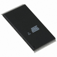
AT49BV802D-70TU Atmel, AT49BV802D-70TU Datasheet

AT49BV802D-70TU
Specifications of AT49BV802D-70TU
Available stocks
Related parts for AT49BV802D-70TU
AT49BV802D-70TU Summary of contents
Page 1
... The x16 data appears on I/O0 - I/O15; the x8 data appears on I/O0 - I/O7. The memory is divided into 23 sec- tors for erase operations. The AT49BV802D(T) is offered in a 48-lead TSOP and a 48-ball CBGA package. The device has CE and OE control signals to avoid any bus contention ...
Page 2
... Pin Configurations Pin Name A0 - A18 RESET RDY/BUSY I/O0 - I/O14 I/O15 (A-1) BYTE NC AT49BV802D(T) 2 Function Addresses Chip Enable Output Enable Write Enable Reset READY/BUSY Output Data Inputs/Outputs I/O15 (Data Input/Output, Word Mode) A-1 (LSB Address Input, Byte Mode) Selects Byte or Word Mode ...
Page 3
... The addressing shown above should be used when the device is operating in the word (x16) mode the byte (x8) mode, A-1 should be used when addressing the protection register: with A the LSB of the address location can be accessed; and with A the MSB of the address location can be accessed. AT49BV802D(T) 14 *NOTICE: Stresses beyond those listed under “Absolute Maximum Ratings” ...
Page 4
... Refer to AC programming waveforms can 12.0V ± 0.5V Manufacturer Code: 1FH (x8); 001FH (x16), Device Code: C1H (x8) - AT49BV802D; 01C1H (x16) - AT49BV802D; C3H (x8) - AT49BV802DT; 01C3H (x16) - AT49BV802DT. 5. Additional device code: 01H (x8) - AT49BV802D(T); 0001H (x16) - AT49BV802D(T). 6. See details under “Software Product Identification Entry/Exit” Ind RESET ...
Page 5
... Programming Current CC1 CC V Input Low Voltage IL V Input High Voltage IH V Output Low Voltage OL1 V Output Low Voltage OL2 V Output High Voltage OH1 V Output High Voltage OH2 Note the erase mode mA. CC AT49BV802D(T) 18 Condition Min I 0. MHz OUT 2 2 1.0 mA ...
Page 6
... DF 4. This parameter is characterized and is not 100% tested. (1)(2)(3)( ADDRESS VALID ACC t RO HIGH after the address transition without impact on t ACC after the falling edge of CE without impact AT49BV802D(T) AT49BV802D(T)-70 Min Max 100 OUTPUT VALID . ACC after an address change CE ACC ...
Page 7
... Input Test Waveforms and Measurement Level 17. Output Test Load 18. Pin Capacitance ( MHz 25°C Symbol Typ OUT Note: 1. This parameter is characterized and is not 100% tested. AT49BV802D( < Max Units Conditions OUT ...
Page 8
... Address Hold Time AH t Chip Select Setup Time CS t Chip Select Hold Time CH t Write Pulse Width ( Write Pulse Width High WPH t Data Setup Time Data, OE Hold Time DH OEH 20. AC Byte/Word Load Waveforms 20.1 WE Controlled 20.2 CE Controlled AT49BV802D(T) Min Max Units ...
Page 9
... For chip erase, the address should be 555. For sector erase, the address depends on what sector erased. (See note 3 under “Command Definition Table” on page 3. For chip erase, the data should be 10H, and for sector erase, the data should be 30H. AT49BV802D(T) 22 PROGRAM CYCLE t ...
Page 10
... Active Standby 70 25 0.025 48C19 48-ball, Plastic Chip-Size Ball Grid Array Package (CBGA) 48T 48-lead, Plastic Thin Small Outline Package (TSOP) Ordering Code Package AT49BV802D-70CU AT49BV802D-70TU AT49BV802DT-70CU AT49BV802DT-70TU Package Type AT49BV802D(T) Operation Range 48C19 Industrial 48T (-40° to 85° C) 48C19 Industrial 48T (-40° ...
Page 11
... E is 0.15 mm per side and 0.25 mm per side. 3. Lead coplanarity is 0.10 mm maximum. 2325 Orchard Parkway San Jose, CA 95131 R PIN SEATING PLANE A1 TITLE 48T, 48-lead ( Package) Plastic Thin Small Outline Package, Type I (TSOP) AT49BV802D(T) 0º ~ 8º GAGE PLANE COMMON DIMENSIONS (Unit of Measure = mm) MIN NOM MAX SYMBOL A – – ...


