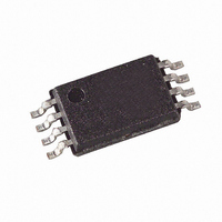
AT34C02-10TU-1.8 Atmel, AT34C02-10TU-1.8 Datasheet - Page 3

AT34C02-10TU-1.8
Manufacturer Part Number
AT34C02-10TU-1.8
Description
IC EEPROM 2KBIT 400KHZ 8TSSOP
Manufacturer
Atmel
Datasheet
1.AT34C02-10PC.pdf
(21 pages)
Specifications of AT34C02-10TU-1.8
Format - Memory
EEPROMs - Serial
Memory Type
EEPROM
Memory Size
2K (256 x 8)
Speed
100kHz, 400kHz
Interface
I²C, 2-Wire Serial
Voltage - Supply
1.8 V ~ 5.5 V
Operating Temperature
-40°C ~ 85°C
Package / Case
8-TSSOP
Lead Free Status / RoHS Status
Lead free / RoHS Compliant
Available stocks
Company
Part Number
Manufacturer
Quantity
Price
Company:
Part Number:
AT34C02-10TU-1.8
Manufacturer:
NVIDIA
Quantity:
10 000
Pin Description
Table 2. AT34C02 Write Protection Modes
Table 3. Pin Capacitance
Applicable over recommended operating range from T
Note:
0958Q–SEEPR–1/07
Symbol
C
C
I/O
IN
1. This parameter is characterized and is not 100% tested.
GND or Floating
GND or Floating
WP Pin Status
Input/Output Capacitance (SDA)
Input Capacitance (A
Test Condition
V
CC
(1)
0
, A
SERIAL CLOCK (SCL): The SCL input is used to positive edge clock data into each
EEPROM device and negative edge clock data out of each device.
SERIAL DATA (SDA): The SDA pin is bidirectional for serial data transfer. This pin is
open-drain driven and may be wire-ORed with any number of other open-drain or open
collector devices.
DEVICE/PAGE ADDRESSES (A2, A1, A0): The A2, A1, and A0 pins are device
address inputs that are hardwired (directly to GND or to Vcc) for compatibility with other
AT24Cxx devices. When the pins are hardwired, as many as eight 2K devices may be
addressed on a single bus system. (Device addressing is discussed in detail under
“Device Addressing,” page 9.) A device is selected when a corresponding hardware and
software match is true. If these pins are left floating, the A2, A1, and A0 pins will be
internally pulled down to GND. However, due to capacitive coupling that may appear
during customer applications, Atmel recommends always connecting the address pins
to a known state. When using a pull-up resistor, Atmel recommends using 10kΩ or less.
WRITE PROTECT (WP): The write protect input, when connected to GND, allows nor-
mal write operations. When WP is connected directly to Vcc, all write operations to the
memory are inhibited. If the pin is left floating, the WP pin will be internally pulled down
to GND. However, due to capacitive coupling that may appear during customer applica-
tions, Atmel recommends always connecting the WP pins to a known state. When using
a pull-up resistor, Atmel recommends using 10kΩ or less.
1
, A
2
, SCL)
Write Protect Register
Not Programmed
Programmed
A
= 25°C, f = 1.0 MHz, V
–
CC
Max
8
6
= +1.8V
Part of the Array Write Protected
Normal Read/Write
First-Half of Array
(1K: 00H - 7FH)
Full Array (2K)
Units
pF
pF
Conditions
V
V
I/O
IN
= 0V
= 0V
3


