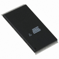
AT49SV802A-90TU Atmel, AT49SV802A-90TU Datasheet - Page 4

AT49SV802A-90TU
Manufacturer Part Number
AT49SV802A-90TU
Description
IC FLASH 8MBIT 90NS 48TSOP
Manufacturer
Atmel
Datasheet
1.AT49SV802A-90CU.pdf
(31 pages)
Specifications of AT49SV802A-90TU
Format - Memory
FLASH
Memory Type
FLASH
Memory Size
8M (1M x 8 or 512K x 16)
Speed
90ns
Interface
Parallel
Voltage - Supply
1.65 V ~ 1.95 V
Operating Temperature
-40°C ~ 85°C
Package / Case
48-TSOP
Lead Free Status / RoHS Status
Lead free / RoHS Compliant
Available stocks
Company
Part Number
Manufacturer
Quantity
Price
Company:
Part Number:
AT49SV802A-90TU
Manufacturer:
ATMEL
Quantity:
50 000
3. Block Diagram
4. Device Operation
4.1
4.2
4
A0 - A18
Read
Command Sequences
AT49SV802A(T)
Y-DECODER
X-DECODER
ADDRESS
BUFFER
LATCH
INPUT
The AT49SV802A(T) is accessed like an EPROM. When CE and OE are low and WE is high,
the data stored at the memory location determined by the address pins are asserted on the out-
puts. The outputs are put in the high impedance state whenever CE or OE is high. This dual-line
control gives designers flexibility in preventing bus contention.
When the device is first powered on, it will be reset to the read or standby mode, depending
upon the state of the control line inputs. In order to perform other device functions, a series of
command sequences are entered into the device. The command sequences are shown in the
“Command Definition Table” on page 13
codes). The command sequences are written by applying a low pulse on the WE or CE input
with CE or WE low (respectively) and OE high. The address is latched on the falling edge of CE
OUTPUT
BUFFER
COMPARATOR
I/O0 - I/O15/A-1
MEMORY
IDENTIFIER
REGISTER
REGISTER
Y-GATING
STATUS
MAIN
DATA
BUFFER
INPUT
(I/O8 - I/O15 are don’t care inputs for the command
WRITE STATE
COMMAND
REGISTER
MACHINE
VOLTAGE SWITCH
PROGRAM/ERASE
3522E–FLASH–10/07
CE
WE
OE
RESET
BYTE
RDY/BUSY
VCC
GND


