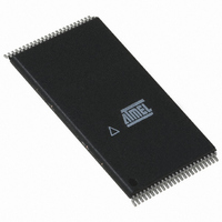
AT49BV163A-70TU Atmel, AT49BV163A-70TU Datasheet - Page 2

AT49BV163A-70TU
Manufacturer Part Number
AT49BV163A-70TU
Description
IC FLASH 16MBIT 70NS 48TSOP
Manufacturer
Atmel
Datasheet
1.AT49BV162A-70TI.pdf
(29 pages)
Specifications of AT49BV163A-70TU
Format - Memory
FLASH
Memory Type
FLASH
Memory Size
16M (2M x 8 or 1M x 16)
Speed
70ns
Interface
Parallel
Voltage - Supply
2.65 V ~ 3.6 V
Operating Temperature
-40°C ~ 85°C
Package / Case
48-TSOP
Lead Free Status / RoHS Status
Lead free / RoHS Compliant
Available stocks
Company
Part Number
Manufacturer
Quantity
Price
Part Number:
AT49BV163A-70TU
Manufacturer:
ATMEL/爱特梅尔
Quantity:
20 000
2. Pin Configurations
2
AT49BV162/163A(T)
The VPP pin provides data protection. When the V
functions are inhibited. When V
be performed.
A six-byte command (Enter Single Pulse Program Mode) sequence to remove the requirement
of entering the three-byte program sequence is offered to further improve programming time.
After entering the six-byte code, only single pulses on the write control lines are required for writ-
ing into the device. This mode (Single Pulse Byte/Word Program) is exited by powering down
the device, or by pulsing the RESET pin low for a minimum of 500 ns and then bringing it back to
V
while in this mode; if entered they will result in data being programmed into the device. It is not
recommended that the six-byte code reside in the software of the final product but only exist in
external programming code.
The BYTE pin controls whether the device data I/O pins operate in the byte or word configura-
tion. If the BYTE pin is set at logic “1”, the device is in word configuration, I/O0 - I/O15 are active
and controlled by CE and OE.
If the BYTE pin is set at logic “0”, the device is in byte configuration, and only data I/O pins I/O0 -
I/O7 are active and controlled by CE and OE. The data I/O pins I/O8 - I/O14 are tri-stated, and
the I/O15 pin is used as an input for the LSB (A-1) address function.
Note:
Pin Name
A0 - A19
CE
OE
WE
RESET
RDY/BUSY
VPP
I/O0 - I/O14
I/O15 (A-1)
BYTE
NC
CC
. Erase, Erase Suspend/Resume and Program Suspend/Resume commands will not work
(1)
1. The V
PP
pin is not available for the AT49BV163A(T).
Function
Addresses
Chip Enable
Output Enable
Write Enable
Reset
READY/BUSY Output
Write Protection
Data Inputs/Outputs
I/O15 (Data Input/Output, Word Mode)
A-1 (LSB Address Input, Byte Mode)
Selects Byte or Word Mode
No Connect
PP
is at 0.9V or above, normal program and erase operations can
PP
input is below 0.4V, the program and erase
3349H–FLASH–3/05


