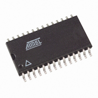
AT45DB321C-RU Atmel, AT45DB321C-RU Datasheet - Page 4

AT45DB321C-RU
Manufacturer Part Number
AT45DB321C-RU
Description
IC FLASH 32MBIT 40MHZ 28SOIC
Manufacturer
Atmel
Datasheet
1.AT45DB321C-RU.pdf
(40 pages)
Specifications of AT45DB321C-RU
Format - Memory
FLASH
Memory Type
DataFLASH
Memory Size
32M (8192 pages x 528 bytes)
Speed
40MHz
Interface
SPI, 3-Wire Serial
Voltage - Supply
2.7 V ~ 3.6 V
Operating Temperature
-40°C ~ 85°C
Package / Case
28-SOIC (7.5mm Width)
Lead Free Status / RoHS Status
Lead free / RoHS Compliant
Available stocks
Company
Part Number
Manufacturer
Quantity
Price
Company:
Part Number:
AT45DB321C-RU
Manufacturer:
ATMEL
Quantity:
8
Part Number:
AT45DB321C-RU
Manufacturer:
ATMEL/爱特梅尔
Quantity:
20 000
5. Device Operation
5.1
5.1.1
4
Read Commands
AT45DB321C
Continuous Array Read
The device operation is controlled by instructions from the host processor. The list of instructions
and their associated opcodes are contained in Tables 1 through 4. A valid instruction starts with
the falling edge of CS followed by the appropriate 8-bit opcode and the desired buffer or main
memory address location. While the CS pin is low, toggling the SCK pin controls the loading of
the opcode and the desired buffer or main memory address location through the SI (serial input)
pin. All instructions, addresses, and data are transferred with the most significant bit (MSB) first.
Buffer addressing is referenced in the datasheet using the terminology BFA9-BFA0 to denote
the 10 address bits required to designate a byte address within a buffer. Main memory address-
ing is referenced using the terminology PA12-PA0 and BA9-BA0, where PA12-PA0 denotes the
13 address bits required to designate a page address and BA9-BA0 denotes the 10 address bits
required to designate a byte address within the page.
By specifying the appropriate opcode, data can be read from the main memory or from either
one of the two SRAM data buffers. The DataFlash supports RapidS protocol for Mode 0 and
Mode 3. Please refer to the “Detailed Bit-level Read Timing” diagrams in this datasheet for
details on the clock cycle sequences for each mode.
By supplying an initial starting address for the main memory array, the Continuous Array Read
command can be utilized to sequentially read a continuous stream of data from the device by
simply providing a clock signal; no additional addressing information or control signals need to
be provided. The DataFlash incorporates an internal address counter that will automatically
increment on every clock cycle, allowing one continuous read operation without the need of
additional address sequences. To perform a continuous read, an opcode of E8H must be
clocked into the device. The opcode is followed by three address bytes (which comprises 24-bit
page and byte address sequence) and 32 don’t care clock cycles. The first bit of the 24-bit
address sequence is reserved for upward and downward compatibility to larger and smaller den-
sity devices (see the notes under
24-bit address sequence specify which page of the main memory array to read, and the last
10 bits (BA9-BA0) of the 24-bit address sequence specify the starting byte address within the
page. The 32 don’t care clock cycles that follow the four address bytes are needed to initialize
the read operation. Following the don’t care clock cycles, additional clock pulses on the SCK pin
will result in data being output on the SO (serial output) pin.
The CS pin must remain low during the loading of the opcode, the address bytes, the don’t care
bytes, and the reading of data. When the end of a page in main memory is reached during a
Continuous Array Read, the device will continue reading at the beginning of the next page with
no delays incurred during the page boundary crossover (the crossover from the end of one page
to the beginning of the next page). When the last bit in the main memory array has been read,
the device will continue reading back at the beginning of the first page of memory. As with cross-
ing over page boundaries, no delays will be incurred when wrapping around from the end of the
array to the beginning of the array.
A low-to-high transition on the CS pin will terminate the read operation and tristate the output pin
(SO). The maximum SCK frequency allowable for the Continuous Array Read is defined by the
f
tents of the buffers unchanged.
CAR
specification. The Continuous Array Read bypasses both data buffers and leaves the con-
Section 13.6 on page
25. The next 13 bits (PA12-PA0) of the
3387M–DFLASH–2/08


