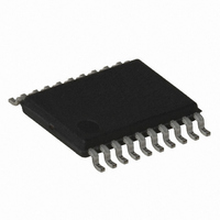
AT27LV520-70XU Atmel, AT27LV520-70XU Datasheet - Page 3

AT27LV520-70XU
Manufacturer Part Number
AT27LV520-70XU
Description
IC OTP 512KBIT 70NS 20TSSOP
Manufacturer
Atmel
Datasheet
1.AT27LV520-90XU.pdf
(13 pages)
Specifications of AT27LV520-70XU
Format - Memory
EPROMs
Memory Type
OTP EPROM
Memory Size
512K (64K x 8)
Speed
70ns
Interface
Parallel
Voltage - Supply
3 V ~ 3.6 V, 4.5 V ~ 5.5 V
Operating Temperature
-40°C ~ 85°C
Package / Case
20-TSSOP
Lead Free Status / RoHS Status
Lead free / RoHS Compliant
3. System Considerations
4. Block Diagram
5. Absolute Maximum Ratings*
Note:
0911G–EPROM–8/07
Temperature under Bias ................................ -55°C to +125°C
Storage Temperature ..................................... -65°C to +150°C
Voltage on Any Pin with
Respect to Ground .........................................-2.0V to +7.0V
Voltage on A9 with
Respect to Ground ......................................-2.0V to +14.0V
V
Respect to Ground .......................................-2.0V to +14.0V
PP
Supply Voltage with
1. Minimum voltage is -0.6V DC which may undershoot to -2.0V for pulses of less than 20 ns. Maximum output pin voltage is
V
CC
+ 0.75V DC which may overshoot to +7.0V for pulses of less than 20 ns.
Switching under active conditions may produce transient voltage excursions. Unless accommo-
dated by the system design, these transients may exceed datasheet limits, resulting in device
non-conformance. At a minimum, a 0.1 µF high frequency, low inherent inductance, ceramic
capacitor should be utilized for each device. This capacitor should be connected between the
V
bilize the supply voltage level on printed circuit boards with large EPROM arrays, a 4.7 µF bulk
electrolytic capacitor should be utilized, again connected between the V
nals. This capacitor should be positioned as close as possible to the point where the power
supply is connected to the array.
CC
and Ground terminals of the device, as close to the device as possible. Additionally, to sta-
AD7 - AD0
A15 - A8
OE/VPP
GND
VCC
ALE
(1)
(1)
(1)
8
PROGRAM LOGIC
OE, ALE, AND
*NOTICE:
Y DECODER
X DECODER
Stresses beyond those listed under “Absolute
Maximum Ratings” may cause permanent dam-
age to the device. This is a stress rating only and
functional operation of the device at these or any
other conditions beyond those indicated in the
operational sections of this specification is not
implied. Exposure to absolute maximum rating
conditions for extended periods may affect device
reliability.
IDENTIFICATION
CELL MATRIX
Y-GATING
BUFFERS
OUTPUT
8
CC
AT27LV520
and Ground termi-
3


