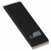
AT49LW080-33TC Atmel, AT49LW080-33TC Datasheet - Page 13

AT49LW080-33TC
Manufacturer Part Number
AT49LW080-33TC
Description
IC FLASH 8MBIT 33MHZ 32TSOP
Manufacturer
Atmel
Datasheet
1.AT49LW080-33JC.pdf
(34 pages)
Specifications of AT49LW080-33TC
Format - Memory
FLASH
Memory Type
FLASH
Memory Size
8M (1M x 8)
Speed
33MHz
Interface
Parallel
Voltage - Supply
3 V ~ 3.6 V
Operating Temperature
0°C ~ 85°C
Package / Case
32-TSOP
Lead Free Status / RoHS Status
Contains lead / RoHS non-compliant
Available stocks
Company
Part Number
Manufacturer
Quantity
Price
Company:
Part Number:
AT49LW080-33TC
Manufacturer:
SST
Quantity:
10 914
Part Number:
AT49LW080-33TC
Manufacturer:
ATMEL/爱特梅尔
Quantity:
20 000
6.7
6.7.1
6.7.2
1966G–FLASH–3/05
Register-based Locking and General-purpose Input Registers
Registers
Sector-locking Registers
may be resumed to successfully complete the program or erase operation. The new lock status
will take place after the program or erase operation completes.
These pins function in combination with the register-based sector locking (to be explained later).
These pins, when active, will write-protect the appropriate sector(s), regardless of the associ-
ated sector locking registers. (For example, when TBL is active, writing to the top sector is
prevented, regardless of the state of the Write Lock bit for the top sector’s locking register. In
such a case, clearing the write-protect bit in the register will have no functional effect, even
though the register may indicate that the sector is no longer locked. The register may still be set
to read-lock the sector, if desired.)
Table 6-4.
A series of registers are available in the FWH to provide software read and write locking and GPI
feedback. These registers are accessible through standard addressable memory space.
The AT49LW080 has two types of registers: sector-locking registers and general-purpose input
registers. The two types of registers appear at their respective address locations in the 4 GB
system memory map.
The AT49LW080 has 16 (LR0 - LR15) sector-locking registers. Each sector-locking register con-
trols the lock protection for 64K bytes of memory as shown in
registers are accessible through the register memory address shown in the third column of
6-5. The sector-locking registers are read/write as shown in the last column of
sector has three dedicated locking bits as shown in
Sector
SA10
SA11
SA12
SA13
SA14
SA15
SA0
SA1
SA2
SA3
SA4
SA5
SA6
SA7
SA8
SA9
Device Memory Map with FWH Hardware Lock Architecture
Size (Bytes)
64K
64K
64K
64K
64K
64K
64K
64K
64K
64K
64K
64K
64K
64K
64K
64K
Address Range
C0000 - CFFFF
D0000 - DFFFF
A0000 - AFFFF
B0000 - BFFFF
E0000 - EFFFF
F0000 - FFFFF
00000 - 0FFFF
10000 - 1FFFF
20000 - 2FFFF
30000 - 3FFFF
40000 - 4FFFF
50000 - 5FFFF
60000 - 6FFFF
70000 - 7FFFF
80000 - 8FFFF
90000 - 9FFFF
Table 6-6
and
Table
Table
Hardware Write-protect Pin
6-5. The sector-locking
6-7.
AT49LW080
TBL
WP
WP
WP
WP
WP
WP
WP
WP
WP
WP
WP
WP
WP
WP
WP
Table
6-5. Each
Table
13


