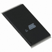
AT49BV163D-70TU Atmel, AT49BV163D-70TU Datasheet - Page 4

AT49BV163D-70TU
Manufacturer Part Number
AT49BV163D-70TU
Description
IC FLASH 16MBIT 70NS 48TSOP
Manufacturer
Atmel
Datasheet
1.AT49BV163D-70CU.pdf
(27 pages)
Specifications of AT49BV163D-70TU
Format - Memory
FLASH
Memory Type
FLASH
Memory Size
16M (2M x 8 or 1M x 16)
Speed
70ns
Interface
Parallel
Voltage - Supply
2.65 V ~ 3.6 V
Operating Temperature
-40°C ~ 85°C
Package / Case
48-TSOP
Lead Free Status / RoHS Status
Lead free / RoHS Compliant
Available stocks
Company
Part Number
Manufacturer
Quantity
Price
Company:
Part Number:
AT49BV163D-70TU
Manufacturer:
ATMEL
Quantity:
4 430
Part Number:
AT49BV163D-70TU
Manufacturer:
ATMEL/爱特梅尔
Quantity:
20 000
4.4
4.4.1
4.4.2
4.5
4.6
4
Erase
Byte/Word Programming
Program/Erase Status
AT49BV163D(T)
Chip Erase
Sector Erase
Before a byte/word can be reprogrammed, it must be erased. The erased state of memory bits is
a logical “1”. The entire device can be erased by using the Chip Erase command or individual
sectors can be erased by using the Sector Erase command.
The entire device can be erased at one time by using the six-byte chip erase software code.
After the chip erase has been initiated, the device will internally time the erase operation so that
no external clocks are required. The maximum time to erase the chip is t
If the sector lockdown has been enabled, the chip erase will not erase the data in the sector that
has been locked out; it will erase only the unprotected sectors. After the chip erase, the device
will return to the read or standby mode.
As an alternative to a full chip erase, the device is organized into 39 sectors (SA0 - SA38) that
can be individually erased. The Sector Erase command is a six-bus cycle operation. The sector
address is latched on the falling WE edge of the sixth cycle while the 30H data input command is
latched on the rising edge of WE. The sector erase starts after the rising edge of WE of the sixth
cycle. The erase operation is internally controlled; it will automatically time to completion. The
maximum time to erase a sector is t
enabled, the sector will erase (from the same Sector Erase command). An attempt to erase a
sector that has been protected will result in the operation terminating immediately.
Once a memory block is erased, it is programmed (to a logical “0”) on a byte-by-byte or on a
word-by-word basis. Programming is accomplished via the internal device command register
and is a four-bus cycle operation. The device will automatically generate the required internal
program pulses.
Any commands written to the chip during the embedded programming cycle will be ignored. If a
hardware reset happens during programming, the data at the location being programmed will be
corrupted. Please note that a data “0” cannot be programmed back to a “1”; only erase opera-
tions can convert “0”s to “1”s. Programming is completed after the specified t
Data Polling feature or the Toggle Bit feature may be used to indicate the end of a program
cycle. If the erase/program status bit is a “1”, the device was not able to verify that the erase or
program operation was performed successfully.
The device provides several bits to determine the status of a program or erase operation: I/O2,
I/O5, I/O6 and I/O7. The
the function of these bits. To provide greater flexibility for system designers, the
AT49BV163D(T) contains a programmable configuration register. The configuration register
allows the user to specify the status bit operation. The configuration register can be set to one of
two different values, “00” or “01”. If the configuration register is set to “00”, the part will automati-
cally return to the read mode after a successful program or erase operation. If the configuration
register is set to a “01”, a Product ID Exit command must be given after a successful program or
erase operation before the part will return to the read mode. It is important to note that whether
the configuration register is set to a “00” or to a “01”, any unsuccessful program or erase opera-
tion requires using the Product ID Exit command to return the device to read mode. The default
value (after power-up) for the configuration register is “00”. Using the four-bus cycle Set Config-
uration Register command as shown in the
“Status Bit Table” on page 10
SEC
. When the sector programming lockdown feature is not
“Command Definition Table” on page
and the following four sections describe
EC
.
BP
cycle time. The
3590A–FLASH–12/05
11, the value


